J. Cent. South Univ. (2016) 23: 598-603
DOI: 10.1007/s11771-016-3106-0

An analytical model to explore open-circuit voltage of a-Si:H/c-Si heterojunction solar cells
ZHONG Chun-liang(钟春良)1, 2, GENG Kui-wei(耿魁伟)2, LUO Lan-e(罗兰娥)1, YANG Di-wu(杨迪武)1
1. Department of Electronics Science and Information Engineering,
Hunan University of Technology, Zhuzhou 412007, China;
2. school of Electronics and Information Engineering, South China University of Technology,Guangzhou 510640, China
 Central South University Press and Springer-Verlag Berlin Heidelberg 2016
Abstract: The effect of the parameters on the open-circuit voltage, Voc of a-Si:H/c-Si heterojunction solar cells was explored by an analytical model. The analytical results show that VOC increases linearly with the logarithm of illumination intensity under usual illumination. There are two critical values of the interface state density (Dit) for the open-circuit voltage (VOC), Ditcrit,1 and Ditcrit,2 (a few 1010 cm-2·eV-1). VOC decreases remarkably when Dit is higher than Ditcrit,1. To achieve high VOC, the interface states should reduce down to a few 1010 cm-2·eV-1. Due to the difference between the effective density of states in the conduction and valence band edges of c-Si, the open-circuit voltage of a-Si:H/c-Si heterojunction cells fabricated on n-type c-Si wafers is about 22 mV higher than that fabricated on p-type c-Si wafers at the same case. VOC decreases with decreasing the a-Si:H doping concentration at low doping level since the electric field over the c-Si depletion region is reduced at low doping level. Therefore, the a-Si:H layer should be doped higher than a critical value of 5×1018 cm-3 to achieve high VOC.
Key words: solar cells; a-Si:H/c-Si heterojunctions; open-circuit voltage
1 Introduction
Amorphous hydrogenated silicon and crystalline silicon (a-Si:H/c-Si) heterojunctions are of great interest for photovoltaic applications due to the high conversion efficiencies achieved so far up to 23% and the possibility of complete fabrication at low temperature process [1]. The open-circuit voltage VOC is a key parameter for the properties of solar cells. VOC is affected by many parameters of solar cells, such as interface states and the doping level of the a-Si:H layer. In particular, the suppression of carrier recombination at the a-Si:H/c-Si heterojunction interface is crucial to improve the open-circuit voltage. Surface passivations [2-5], such as using hydrofluoric acid-based solutions, had been proposed to reduce interface recombination in the past two decades. In the recent decade, the use of a thin intrinsic a-Si:H buffer layer between the emitter and the wafer was proposed to decrease interface states [6-8]. The passivation of c-Si surfaces by an intrinsic a-Si:H ((i) a-Si:H) layer leads to very low effective surface recombination velocities [9]. Sanyo used the passivation property of (i) a-Si:H in their so-called HIT structure solar cell consisting of (p+) a-Si:H/(i) a-Si:H/(n) c-Si/(i) a-Si:H/(n+) a-Si:H. high open-circuit voltage of more than 720 mV was achieved with conversion efficiencies higher than 23.0%. It is usually assumed that interface states should reduce down to very low levels in order to achieve high VOC as well as high conversion efficiency.
Effect of other parameters on the open-circuit voltage, such as the doping concentration of a-Si:H layer and the illumination intensity, was widely investigated by experiments and simulations [10-12]. VOC decreases with decreasing the doping level of the a-Si:H layer in Ref. [11]. However, the quantitative relation between the open circuit voltage and parameters is not clear, and needs to further study. Furthermore, the effect of some other parameters on the open-circuit voltage of a-Si:H/c-Si heterojunction solar cells is obscure. VOC is different from the polarity of the c-Si wafer type [13-15]. HIT solar cells fabricated on n-type c-Si wafers achieve VOC higher than 720 mV [1], while the one on p-type c-Si wafers is about 680 mV. And a-Si:H/c-Si heterojunction solar cells without the (i) a-Si:H layer fabricated on n-type c-Si wafers achieved VOC of about 640 mV whereas on p-type c-Si wafers was about 629 mV [16]. However, higher VOC of a-Si:H/c-Si heterojunction solar cells fabricated on p-type c-Si wafers with higher efficiency was found [17-18]. It seems to be contradictory. Therefore, it is indispensible to further investigate the observed effect, especially combining with an analytical model of the open-circuit voltage for a-Si:H/c-Si heterojunction solar cells. Recently, an analytical model of the open-circuit voltage for silicon heterojunction solar cells is derived by integrating the equation of the electron current density at the depletion region and solving the excess density at c-Si under illumination and open-circuit [19]. In this work, the analytical model of the open circuit voltage was applied to various cases, such as the interface state intensity, the polarity of the c-Si wafer type and the a-Si:H doping concentration to quantitatively explore effect of the parameters on the open- circuit voltage.
2 Experimental and simulation details
To explore effect of the parameters on the open- circuit voltage of a-Si:H/c-Si heterojunction solar cells, a set of simulations were performed, and (n+) a-Si:H/(p) c-Si heterojunction solar cells were fabricated. Heterojunction solar cells were fabricated by PECVD deposition of n-type a-Si:H layer onto p-type crystalline Si substrate (FZ, 1-5 Ω·cm, (111), 300 μm) with back surface field at a substrate temperature of 200 °C. The thickness of the (n+) a-Si:H emitter was about 10 nm. Before the thin film deposition, the c-Si wafers were prepared by removing the native oxide using a wet chemical etching procedure (HF diluted at 5% in water). Contact to the a-Si:H emitter was made by a 80 nm thick ITO deposited by magnetron sputtering. Evaporated aluminium was used for the grid and rear contacts. I-V characteristics were measured under various illumination intensities at 300 K.
A set of simulations were performed using the AFORS-HET v.2.2 program [20]. We changed Dit in the range of 1×10⁹ -4×1012 cm-2·eV-1 and ND2 in the range of 1×10¹⁸-2×1019 cm-3. The density of gap states (DOS) was adopted for a-Si:H. It consisted of two exponential band tails with characteristic energies of 0.036 eV and 0.05 eV for the conduction and valence band, respectively, and with a pre-exponential factor of 1×1021 cm-3·eV-1, and two Gaussian deep defect distributions of donor and acceptor natures being located at 0.6 eV and 0.7 eV above the maximum valence band, respectively, with a maximum value of 2.4×1019 cm-3·eV-1 and a standard deviation of 0.15 eV [21]. The DOS at the Fermi level was equal to 1019 cm-3·eV-1. The interface is described by introducing a very thin defective c-Si interface layer between a-Si:H and c-Si. The defect distribution in this interface layer is taken as constant through the band gap, assuming donor/acceptor-like defects in the lower/upper part of the band gap. These material parameters of the c-Si and a-Si:H layers are given in Table 1 for the numerical simulations. All the results presented in this work from numerical simulation were obtained at 300 K under AM1.5 illumination.
Table 1 Main parameters of a-Si:H/c-Si heterojunction layers used in simulations

3 Results and discussion
3.1 Analytical model of open-circuit voltage
By integrating the equation of the electron current density at the depletion region and combining with the band diagram of (n+) a-Si:H/(p) c-Si heterojunctions at equilibrium and under illumination and open-circuit shown in Fig. 1, an analytical model of the open circuit voltage for (n+) a-Si:H/(p) c-Si heterojunction solar cells is given by [19]
 (1)
(1)
where β=kT/q, Eg1 is the band gap of c-Si; Nc1 is the effective density of states in the conduction band edge of c-Si; np0 and nn0 are the free electron densities at neutral regions of the c-Si at the thermal equilibrium; △n(xp) is the excess of the carriers at the boundary of the c-Si depletion region (x=xp); and δp1 is the activation energy of p-type c-Si wafers, which can be deduced from the doping impurity concentration of the substrate, NA1. Deduced from Eq. (1), VOC is related with △n(xp). By solving the hole continuity equation under illumination and open circuit, the excess electron density at x=xp under a low-injection condition is given by [22]
 (2)
(2)
where △n=gτeff (g is the average photogeneration of the electron-hole pairs in c-Si; τeff is the effective lifetime of the excess carries); the interface recombination velocity for holes is Sp=CpDit; the diffusion length of holes is Lp=(Dpτeff)1/2; Cp is the capture rate coefficient; and Dp is the hole diffusion constant. Substituting Eq. (2) into Eq.(1) and neglecting np0 ( ), the open-circuit voltage of (n) a-Si:H/(p) c-Si heterojunction solar cells is given by
 (3)
(3)
Similarly, the open-circuit voltage of (p) a-Si:H/(n) c-Si heterojunction solar cells is given by
 (4)
(4)
where δn1 is the activation energy of n-type c-Si wafers; Sn is the interface recombination velocity for electrons; Ln is the diffusion length of electrons; and NV1 is the effective density of states in the valence band edge of c-Si.
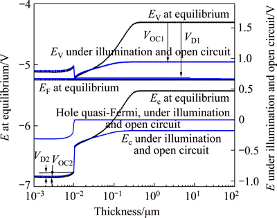
Fig. 1 Energy band diagram of (n) a-Si:H/(p) c-Si heterojunctions at equilibrium (black lines) and under illumination and open circuit (blue lines) (where VD1 and VD2 are the diffusion potentials on c-Si and a-Si:H layers, respectively; and VOC1 and VOC2 are photogenerated potentials on the c-Si and a-Si:H layers, respectively)
Deduced from the analytical model of the open- circuit voltage (Eq. (3) and Eq. (4)), VOC mostly depends on the activation energy of the c-Si substrate, δp1 or δn1 (or the doping concentration of the c-Si substrate), the interface state density, Dit, the average photogeneration of the electron-hole pairs g, the effective lifetime of the excess carries, τeff, and the diffusion length Lp or Ln. τeff and Lp (or Ln) are linked to the recombination velocities at the heterojunction interface, at the rear surface and in the bulk. g is related with the illumination intensity. Therefore, the open-circuit voltage mostly depends on the interface state density, the illumination intensity, the recombination velocities at the rear surface and in the bulk, and the activation energy of the c-Si substrate. And it is apparently independent on the a-Si:H doping concentration.
3.2 Application of analytical model of open circuit voltage
Figure 2 shows the dependence of the illumination intensity on the open-circuit voltage of a-Si:H/c-Si heterojunction solar cells fabricated, where the irradiance of 100 mW/cm2 corresponds to one-sun irradiance. As τeff can be approximately assumed constant under usual illumination [7], Eq. (3) reduces to
 (5)
(5)
where  is the open-circuit voltage at one-sun irradiance (X=1). The theoretical dependence of VOC on the illumination intensity, which is deduced from Eq. (5), is also shown in Fig. 2. it is in accordance with the experimental curve. Deduced from Eq. (5), VOC increases linearly with the logarithm of X under usual illumination.
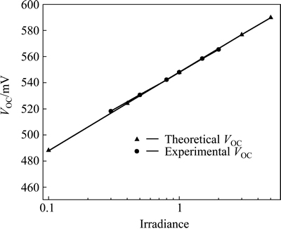
Fig. 2 Experimental VOC and theoretical VOC of a-Si:H/c-Si heterojunction solar cells under various illumination intensity
The dependence of the simulated open-circuit voltage, VOCsim, on Dit is shown in Fig. 3. Simultaneously, the curve of the theoretical open-circuit voltage VOCCal versus Dit is also plotted in Fig. 3, where VOCCal are calculated from Eq. (1) and △n(xp) is shown in Fig.4. Seen from Fig. 3, the curve of VOCcal is in accordance with the VOCsim. And the dependence of the open-circuit voltage is divided into three zones, and there are two critical values of Dit for VOC, Ditcrit,1 and Ditcrit,2. For very low values of Dit (Dit≤Ditcrit, 2), VOC does not almost depend on Dit. By increasing Dit from Ditcrit,2 to Ditcrit,1, VOC decreases, and further increasing Dit at Dit> Ditcrit,1 leads to a dramatic decrease of VOC.
Deduced from Eq. (3), the effect of interface states on the open-circuit voltage of a-Si:H/c-Si heterojunction solar cells is related with the parameter △n (gτeff). The simulated values of △n under illumination and open circuit for different values of Dit are shown in Fig. 4. It is known that τeff is determined by the interface recombination velocity and the recombination velocities in the c-Si bulk and at the rear contact of solar cells. As the recombination velocities in the c-Si bulk and at the rear contact may be dominant comparable with Sp at Dit≤Ditcrit,1, τeff is almost not affected by Dit. It results in △n keeping unchanged. However, as Sp may be comparable or dominant above Ditcrit,1, τeff decreases with increasing Dit. It results in △n decreasing.
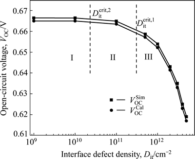
Fig. 3 Simulated and theoretical dependences of VOC of (n+) a-Si:H/(p) c-Si heterojunction solar cells on Dit
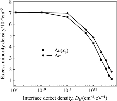
Fig. 4 free excess electron density at x=xp, △n(xp), and excess electron density out of c-Si depletion and diffusion regions, △n, under illumination and at open circuit for various Dit
There is another critical value of Dit for Dp/Lp, Ditcrit,2. When Dit ≤Ditcrit,2, since △n is independent on Dit, and simultaneously Sp is small enough to neglect comparing with Dp/Lp, VOC is almost independent of Dit. When Ditcrit,2< Dit ≤Ditcrit,1, Sp is comparable with Dp/Lp, and increases with increasing Dit, while △n keeps unchanged, and it results in VOC decreasing. Further increasing Dit when Dit> Ditcrit,1, Sp increases with Dit, and furthermore △n decreases with Dit. It results in a dramatic decrease of VOC.
Ditcrit,1 is dependent on the recombination velocities in the c-Si bulk and at the rear contact of solar cells. The second critical value of Dit is Ditcrit, 2. Equation (3) reduces to
 (6)
(6)
with
 and
and 
where β=26 mV at 300 K, and Dp is 13 cm2/s. Ditcrit,2 is dependent on Dp/Lp. Since Ditcrit,2itcrit,1, Lp and then Ditcrit,2 are dependent on the recombination velocity in the c-Si bulk. The dependence of Φ versus α is shown in Table 2. Seen from Table 2, the ratio of Sp to Dp/Lp, α, should decrease down to 0.1 in order to achieve high value of VOC. Deduced from the simulated Internal quantum efficiency measurement, Lp=1.21×10⁻² cm. The critical value of Sp is about 100 cm/s. And Ditcrit,2 is usually a few 1010 cm-2·eV-1. Therefore, the interface states should reduce down to a few 1010 cm-2·eV-1 to achieve high VOC as well as high performance of a-Si:H/c-Si heterojunction solar cells. To reduce interface states lower than Ditcrit,2, the passivation of a thin intrinsic a-Si:H layer introduced between the emitter and the wafer was proposed by Sayno. It leads to very low effective interface recombination velocity of 3 cm/s. The interface states (or the interface recombination velocity) are lower than the critical value Ditcrit,2. The solar cell achieved high efficiency with the open-circuit voltage higher than 720 mV. Therefore, the i-a-Si:H buffer layer mainly plays the role of interface passivation in decreasing interface states. To achieve high performance of a-Si:H/c-Si heterojunction solar cells, it is usually assumed that interface states should reduce down to very low levels as possible. Deduced from the analytical model of the open-circuit voltage, when the interface states are lower than Ditcrit,2, it is of no great significance to further decrease the interface states to improve the open-circuit voltage.
Table 2 Dependence of Φ on α
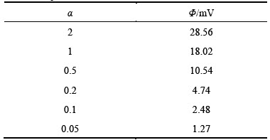
Figure 5 shows the simulated I-V characteristics of a-Si:H/c-Si heterojunction solar cells fabricated on both p- and n-type c-Si wafers with the same activation energy of c-Si (δp1=δn1) and the same value of the interface recombination velocity. Seen from Fig. 7, the open-circuit voltage of a-Si:H/c-Si heterojunction solar cells fabricated on n-type c-Si wafers is about 22 mV higher than that fabricated on p-type c-Si wafers. The discrepancy is in accordance with the value deduced from the analytical model of the open-circuit voltage Eq. (3) and Eq. (4). The discrepancy origins from the difference of Nc1 and NV1 (Nc1=2.80×1019 cm-3 and NV1=1.04×1019 cm-3). Therefore, n-type c-Si wafers have superiority to achieve higher values of VOC as well as higher performance of a-Si:H/c-Si heterojunction solar cells.
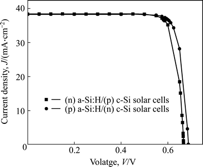
Fig. 5 J-V characteristics of (n) a-Si:H/(p) c-Si and (p) a-Si:H/(n) heterojunction solar cells
The simulated dependence of VOC on the a-Si:H doping concentration ND2 is shown in Fig. 6. Seen from Fig. 6, VOC decreases with decreasing the doping level of the a-Si:H layer at low doping levels (ND2 < 5×1018 cm-3) as it was reported in Ref. [11]. It seems to contradict with Eq. (3). In fact, at low doping levels, the depletion region has shift towards the a-Si:H layer. The diffusion voltage is mainly distributed over the a-Si:H layer. The electric field over the c-Si depletion region is strongly reduced. It allows more holes to diffuse from the c-Si neutral region towards the heterojunction interface. Higher hole concentration in the c-Si depletion region in combination with the high accumulation of electrons near theinterface causes a strong increase of the interface recombination. Deduced from Eq. (3), it results in the decrease of VOC at low doping levels.
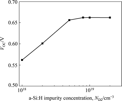
Fig. 6 Simulated dependence of VOC on a-Si:H impurity concentration ND2.
However, at a high doping levels (ND2>5×1018 cm-3), VOC is independent on ND2. It is in accordance with Eq. (3). For a-Si:H/(p) c-Si heterojunction solar cells with high doping levels, the total diffusion potential is mainly accommodated in the c-Si. Only a small fraction of the total diffusion potential is accommodated inside the (n+) a-Si:H layer so that it can be neglected. It results in low interface recombination, and then high value of VOC. Therefore, to achieve high VOC as well as high performance of a-Si:H/c-Si heterojunction solar cells, the a-Si:H layer should be doped higher than 5×1018 cm-3.
4 Conclusions
Effect of the parameters on the open-circuit voltage was explored by an analytical model. The analytical results show that VOC increases linearly with the logarithm of illumination intensity under usual illumination. And n-type c-Si wafers have superiority to achieve higher values of VOC as well as higher performance of a-Si:H/c-Si heterojunction solar cells. To achieve high VOC as well as high performance of a-Si:H/c-Si heterojunction solar cells, the interface states should reduce down to 1010 cm-2·eV-1, and the a-Si:H layer should be doped higher than a critical value of 5×1018 cm-3.
References
[1] Tsunomura Y, Yoshimine Y, Taguchi M, BABA T, KINOSHITA T, KANNO H, SAKATA H, MARUYAMA E, TANAKA M. Twenty-two percent efficiency HIT solar cell [J]. Sol Energy Mater Sol Cells, 2009, 93: 670-673.
[2] Wang T H, Wang Q, Page M R, Bauer R E, Ciszek T F. Hydrogen passivation and junction formation on APIVT-deposited thin-layer silicon by hot-wire CVD [J]. Thin Solid Films, 2003, 430: 261-264.
[3] Ikhmayies S J, Ahmad-Bitar R N. Using HF rather than NH4F as doping source for spray-deposited SnO2:F thin films [J]. Journal of Central South University, 2012, 19(3): 791-796.
[4] Tanaka Y, MatsukiN, Fujiwara H. Characterization ofa-Si:Hthin layers incorporated into textureda-Si:H/c-Si solar cellstructures by spectroscopic ellipsometry usingatilt-angle optical configuration [J]. Thin Solid Films,2014, 569: 64-69.
[5] Pehlivan  , Menda D, YIlmazO,
  A O,
A O,  zdemir O, Duygulu
  , KUTLU K, TOMAK M. Structural and interfacial properties of large area n-a-Si:H/i-a-Si:H/p-c-Siheterojunctionsolar cells [J]. Materials Science in Semiconductor Processing,2014, 22: 69-75
[6] Kim S K, Lee J C, Park S J, Kim Y J, Yoon K H. Effect of hydrogen dilution on intrinsic a-Si:H layer between emitter and Si wafer in silicon heterojunction solar cell [J]. Sol Energy Mater Sol Cells, 2008, 92: 298-301.
[7]  D, Voz C, Martin I, Orpella A, Puigdollers J, Alcubilla R, Villar F, Bertomeu J, Andreu J, Damon-Lacoste J, Roca i Cabarrocas P. Progress in a-Si:H/c-Si heterojunction emitters obtained by Hot-Wire CVD at 200 °C [J]. Thin Solid Films, 2008, 516: 761-764.
[8] Veschetti Y, Muller J C, Damon-Lacoste J, Roca i, Cabarrocas P, Gudovskikh A S, Kleider J P, Ribeyron P J, Rolland E. Optimisation of amorphous and polymorphous thin silicon layers for the formation of the front-side of heterojunction solar cells on p-type crystalline silicon substrates [J]. Thin Solid Films, 2006, 511/512: 543-547.
[9] Dauwe S, Schmidt J, Hezel R. Very low surface recombination velocities on p- and n-type silicon wafers passivated with hydrogenated amorphous silicon films [C]// Conference Record of the Twenty-Ninth IEEE Louisiana. New Orleans: Photovoltaic Specialists Conference, 2002: 1246-1249.
[10] Froitzheim A, Brendel K, Elstner L, Fuhs W, Kliefoth K, Schmidt M. Interface recombination in heterojunctions of amorphous and crystalline silicon [J]. J Non-cryst Solids, 2002, 299/302: 663-667.
[11] van Cleef M W, Rubinelli F A, Rath J K. Photocarrier collection in a-SiC:H/c-Si heterojunction solar cells [J]. J Non-cryst Solids, 1998, 227/230: 1291-1294.
[12] Page M R, Iwaniczko E, Xu Y Q, Roybal L, Hasoon F, Wang Q, Crandall R S. Amorphous/crystalline silicon heterojunction solar cells with varying i-layer thickness [J]. Thin Solid Films, 2011, 519: 4527-4530.
[13] Nath M, Chatterjee P, Damon-Lacoste J, Roca i, Cabarrocas P. Criteria forimproved open-circuit voltage in a-SiH/c-Si(P) front heterojubnction solar cells [J]. J Appl Phys, 2008, 103: 034506.
[14] Wang Q, Page M R, Iwaniczko E, Xu Y Q, Roybal L, Bauer R, To B, Yuan H C, Duda A, Yan Y F. Crystal silicon heterojunction solar cells by hot wire CVD [C]// Proceedings of the 33rd PVSEC-IEEE. San Diego, USA: IEEE, 2008: 1-5.
[15] Damian P P, Bivour M, Hermle M, Stefan W G. Amorphous silicon carbide heterojunction solar cells on p-type substrates [J]. Thin Solid Films, 2011, 519: 2550-2554.
[16] Schmidt M, Korte L, Laades A, Stangl R, Schubert C, Angermann H, Conrad E, Maydell K V. Physical aspects of a-Si:H/c-Si hetero-junction solar cells [J]. Thin Solid Films, 2007, 515: 7475-7480.
[17] Tucci M, della Noce M, Bobeico E, Roca F, de Cesare G, Palma F. Comparison of amorphously crystalline heterojunction solar cells based on n- and p-type crystalline silicon [J]. Thin Solid Films, 2004, 451/452: 355-360.
[18] Voz C,  D, Fonrodona M, Martin I, Puigdollers J, Alcubilla R, Escarre J, Bertomeu J, Andreu J. Bifacial heterojunction silicon solar cells by hot-wire CVD with open-circuit voltages exceeding 600 mv [J]. Thin Solid Films, 2006, 511/512: 415-419.
[19] Zhong C L, Luo L E, Tan H S, Geng K W. Band gap optimization of the window layer in silicon heterojunction solar cells [J]. Solar Energy, 2014, 8: 570-575
[20] Stangl R, Froitzheim A, Kriegel M, Brammer T, Kirste S, Elstner L, Stiebig H, Schmidt M, Fuhs W. AFORS-HET, a numerical PC-program for simulation of heterojunction solar cells, Version 1.1 (open-source on demand), to be distributed for public use [C]// Proc 19th European Photovoltaic. France: Solar Energy Conference, 2004: 1497-1500.
[21] Schmidt M, Schoepke A, Korte L, MLICH O, FUHS W. Density distribution of gap states in extremely thin a-Si:H layers on crystalline silicon wafers [J]. J Non-cryst Solids, 2004, 211: 338-340.
[22] Zhong C L, Yao R H, Geng K W. Characterization of interface states in a-Si-H/c-Si heterojunctions by an expression of the theoretical diffusion capacitance [J]. J Phys D: Appl Phys, 2010, 43: 495102.
(Edited by YANG Hua)
Foundation item: Project(11374094) supported by the National Natural Science Foundation of China; Project(2013HZX23) supported by Natural Science Foundation of Hunan University of Technology, China; Project(2015JJ3060) supported by Natural Science Foundation of Hunan Province of China
Received date: 2014-12-29; Accepted date: 2015-05-25
Corresponding author: ZHONG Chun-liang, PhD, lecturer; Tel +86-15974381036; E-mail: zhongcljust2007@163.com