
Electrochemical modification process of anodic alumina membrane
YU Mei(于 美), LIU Jian-hua(刘建华), LI Song-mei(李松梅)
School of Materials Science and Engineering, Beijing University of Aeronautics and Astronautics, Beijing 100083, China
Received 10 April 2006; accepted 25 April 2006
Abstract: The modification procedure of anodic alumina membrane(AAM) was studied. The AAM structure after modification was characterized by nickel nanowires prepared in AAM. Scanning electron microscopy was used to characterize the topography and structure properties of the AAM and nickel nanowires. The transformation of the current during the voltage reduction was studied. The mechanism of current and structure change during modification was discussed. The results show that a root structure produces after the AAM modification. The length of the root structure depends on the velocity of the voltage reduction. Slow voltage reduction leads to a large length of the root structure, otherwise, a short length of the root structure. At the end of the modification, the barrier layer is thin enough to be passed by electrons. Hence, the direct electrodeposition of one-dimensional nanowires can be carried out on the AAM with barrier layer and aluminum matrix successfully without any other treatments.
Key words: anodic alumina membrane; modification; electrodeposition; nanowires
1 Introduction
The synthesis of one-dimension nanomaterials attracted more and more interests because of their basic concepts and potential technology application, such as high density perpendicular magnetic recording media and nanosensor[1-3]. The AAM played an important role in the synthesis of one-dimension nanomaterials due to their advantages[3,4]. There are many approaches based on AAM to fabricate one-dimension nanomaterials, such as alternating current electrodeposition[5], direct current electrodeposition[6-8], sol-gel[9], electroless deposition[10] and vapor-phase deposition technique[11]. Among the different approaches to the fabrication of one-dimension nanomaterials, direct current electro- deposition based synthetic method was used widely. The ideal AAM consists of three parts of nanopores alumina, barrier layer (in the middle of nanopores alumina and aluminum matrix) and aluminum matrix. The general processes in direct current electrodeposition are that the aluminum matrix is dissolved at first and then etched to remove the compact layer. Then, a conductive metal layer is sputterdeposited on one side of the AAM to serve as the working electrode during the electrodeposition. These processes are inconvenient and the pore diameter of AAM is not easily controlled after the etching.
In this paper, an easy synthesis approach was suggested without removing the barrier layer and aluminum matrix of the AAM before the electrodeposition. The thickness of the barrier layer was modified by additional electrochemical process after completing the anodizing step of the AAM. After the modification of the AAM, the preparation of one-dimension nanomaterials based on direct current electrodeposition was carried out successfully without other treatments. The anodizing voltage of modification processes decreased at a certain velocity. The transformation of the current during the decreasing processes of the voltage was also studied.
Through the modification of the AAM, nickel (Ni) nanowires were prepared successfully using the direct current electrodeposition in the AAM with barrier layer and aluminum substrate without any other treatments. It is known that the topography of the nanowires is similar with the pores of AAM[6, 8, 9]. Therefore, the change of the AAM morphology based on the modification was characterized by that of the nickel nanowires.
2 Experimental
The AAM templates were prepared in 0.3 mol/L oxalic acid solution by a two-step anodizing process[12]. The pure aluminum (Al) sheet (99.999%) plates were degreased in acetone, and then annealed in the furnace at 500 ℃ for 1.5 h to remove the mechanical stress and recrystallize. The Al plates were electropolished under a constant current of 10 mA/cm2 for 1 min. Electropoli- shing solution was a mixture of HClO4 and C2H5OH with the volume ratio of 1∶4.
In the first step of anodic oxidation process, the pretreated aluminum sheets were exposed to the prepared acid solution in the electrochemical cell at voltage of 40 V for 3 h. During anodization, electrochemical cell was put in a water bath to keep temperature at the room temperature. Then, the plates were immersed in a mixture solution of phosphoric acid (0.4 mol/L) and chromic acid (0.2 mol/L) at 60 ℃ for 3 h to remove the alumina layer formed in the first step of anodization process.
The parameters of the second step of anodization processes were the same with that of the first step of anodization process. Between two steps, the alumina plates were washed with distilled water.
After the second step of anodizing procedure, the modification process was carried out by decreasing the anodizing voltage at 1-1.5 V/s. The decreasing process of the voltage was not stopped until the anodizing voltage was smaller than the electrodeposition voltage applied. And also, the anodizing voltage was separately reduced from 40 V to 35 V (sample A) and from 40 V to 30 V (sample B) to study the change of the current with the reduction of anodizing voltage.
The direct current electrodeposition of the nickel nanowires was performed in a bath containing NiSO4 (200 g/L), NiCl (50 g/L), H3BO3 (45 g/L) at the room temperature after the AAM modification. The pH value of the bath was adjusted to 4.4-5.2.
Scanning electron microscopy (SEM XL30 S-FEG) was used to characterize the topography and structure properties of the AAM and the nickel nanowires. Au nanoparticles were sputtered on the AAM sample surface before SEM measurement and increased the conductivity. The AAM was removed with 6 mol/L NaOH.
3 Results and discussion
Fig.1 shows SEM images of AAM. As shown in Fig.1(a), the AAM has a highly ordered porous structure and the pores organize in an almost precise hexagonal structure. From Fig.1(b), the pores are straight, uniform and parallel to each other in the whole length. The microparticles on the surface shown in the micrograph are Au caused by the sputtering Au before SEM determination. Au microparticles were too large to find the detail of the transformation of the AAM structure after modification. Because the morphology of nanowires prepared by AAM template method was similar with that of the nanopores in the used AAM, the morphology of nickel nanowires was also characterized by SEM to investigate the change of the AAM structure after the modification.
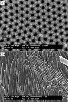
Fig.1 SEM images of AAM: (a) Top-view; (b) Cross-section view
Fig.2 shows the SEM image of nickel nanowires fabricated within the nanopores of AAM after modification of the AAM. Fig.2(b) shows the magnification graph of the nanowires bottom corresponding to Fig.2(a). It is shown that there are many rooted structure at the bottom of nanowires and all the nanowires in area B (marked in Fig.2(a)). But, nanowires in area A (marked in Fig.2(a)) are almost smooth surface contrast to area B. Because the size of the nanowires is similar with that of the used AAM, it can be concluded that the structure of the AAM changes with the procedures of modifying. There are root structures at the base of AAM nanopores.
The transformation of the anodizing current density with the voltage decreasing is shown in Fig.3. It indicates that the current steep reduces when the voltage decreases rapidly from 40 V to 35 V (sample A) and from 40 V to 30 V (sample B) at 60 s. The current comes to stabilization with the anodization process performing. Sample A has a shorter time to reach steady state contrast to sample B.
The changes of the anodizing current and the AAM structure with the voltage reduction were explained by following model[13]. Column (a) is the schematic diagram of barrier layer seen from the arrow as shown in
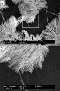
Fig.2 SEM images of Ni nanowires: (a) Large scale area; (b) Magnification graph of area marked in (a)
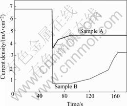
Fig.3 Changes curves of anodizing current with voltage (Sample A from 40 V to 35 V, sample B from 40 V to 30 V)
Fig.4. Column (b) in Fig.4 is the schematic diagram of the AAM cross section. The thickness of the barrier depends on the anodizing voltage (1-1.2 nm/V)[14]. The barrier will dissolve with the anodizing voltage decreasing (step Ⅱ) until the thickness adapts to the later voltage (step Ⅲ). With the barrier dissolving, the new smaller pores are produced at the base of previous larger pores. When the voltage decreases rapidly, the barrier will dissolve, so there are no current flowing in the anodizing electric circuit. It can explain the current changes in Fig.3.
The modification of AAM in this paper is a continuous voltage reduction instead of rapid reduction.
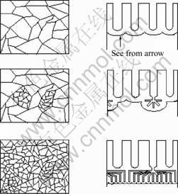
Fig.4 Schematic diagram of AAM change during anodizing voltage reducing
When the voltage decreases at a certain velocity, the barrier is dissolving. Smaller pores are produced at the barrier layer. Then, there are smaller pores produced at the base of the new pores and it causes a root structure at base of pores. Fig.5 illustrates the structure of the pores after AAM modifying and also explains the results of Fig.2. The length of the root structure depends on the velocity of the voltage reduction. High velocity leads to short time modification and short length of the root structure. Otherwise, slow velocity leads to modification of long time and increases the length of the root structure.
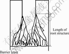
Fig.5 Schematic diagram of AAM structure after modification
The thickness of the barrier layer reduces with the voltage reducing. At the end of AAM modification, the anodizing voltage will be smaller than the voltage planed to apply during electrodeposition. Hence, electron can pass the thin barrier layer at the electric field produced by the electrodeposition voltage when the electro- deposition performs. It also is proved by the successful synthesis of nickel nanowires in our work.
4 Conclusions
The AAM templates are modified successfully by the anodizing voltage reduction. The modification of the nanopores AAM simplifies the synthesis process of one- dimensional nanomaterials. The AAM structure changes after the modification. A root structure produces at the base of the pores. The length of root structure depends on the velocity of the voltage reduction. The thickness of the barrier layer becomes smaller and smaller with the modification process performing. When the electrodeposition voltage planed to apply is larger than the voltage at end of the modification procedure, direct current electrodeposition can perform successfully without any other treatments.
References
[1] YAN T P, GUO W MG, ZHANG L D, SHAN W J, ZHANG CH, GAO X Y, ZHAO A W. Synthesis of ordered Al nanowire arrays [J]. Solid State Sci, 2003, 5: 1063-1067.
[2] FORRER P, SCHLOTTIG F, SIEGENTHALER H, TEXTOR M. Electrochemical preparation and surface properties of gold nanowire arrays formed by the template techniques [J]. J App Electro, 2000, 30: 533-541.
[3] YU C S, JOS? M. S. Characterization of anodic porous alumina by AFM [J]. Mater Lett, 2001, 48: 127-136.
[4] MASUDA H, YAMADA H, SATOH M, ASOH H. Highly ordered nanochannel-array architecture in anodic alumina [J]. Appl Phys Lett, 1997, 71: 2770-2772.
[5] ZONG R L, ZHOU J, LI Q, DU B, LI B, FU M, QI X W, LI L T. Synthesis and optical properties of silver nanowire arrays embedded in anodic alumina membrane [J]. J Phys Chem B, 2004, 108: 16713-16716.
[6] ZHENG M J, ZHANG L D, LI G H, SHEN W Z. Fabrication and optical properties of large-scale uniform zinc oxide nanowire arrays by one-step electrochemical deposition technique [J]. Chemical Physics Letters, 2002, 363: 123-128.
[7] PAN H, LIU B, YI J, POH C, LIM S, DING J, FENG Y, HUAN C H A, LIN J. Growth of single-crystalline Ni and Co Nanowires via electrochemical deposition and their magnetic properties [J]. J Phys Chem B, 2005, 109: 3094-3098.
[8] LI Y, CHENG G S, ZHANG L D. Fabrication of highly ordered ZnO nanowire arrays in anodic alumina membrane [J]. J Mater Res, 2000, 15: 2305-2308.
[9] LIU J H, YU M, LI S M. Preparation and characterization of highly ordered iron oxide nanowire arrays by sol-gel template method [J]. Chinese Journal of Inorganic Chemistry, 2005, 21(3): 429-432.(in Chinese)
[10] MENON V P, MARTIN C R. Fabrication and evaluation of nanoelectrode ensembles [J]. Anal Chem, 1995, 67: 1920-1928.
[11] CHENG G S, ZHANG L D, ZHU Y, FEI G T, LI L, MO C M, MAO Y Q. Large-scale synthesis of single crystalline gallium nitride nanowires [J]. Appl Phys Lett, 1999, 75: 2455-2457.
[12] MASUDA H, FUKUDA K. Ordered metal nanohole arrays made by a two-step replication of honeycomb structures of anodic alumina [J]. Science, 1995, 268: 1466.
[13] ZENG L S. Properties and removing of the anodic alumina membrane [J]. Plating and Finshing, 1997, 19(2): 24-27.
[14] SAEDI A, GHORBANI M. Electrodeposition of Ni-Fe-Co alloy nanowire in modified AAO template [J]. Materials Chemistry and Physics, 2005, 91: 417-423.
(Edited by LI Yan-hong)
Corresponding author: LIU Jian-hua; Tel/Fax: +86-10-82317103; E-mail: liujh@buaa.edu.cn