Cluster-assembled cobalt doped ZnO nanostructured film prepared by low energy cluster beam deposition
ZHAO Shi-feng(赵世峰)1, 2, YAO Chang-hong(姚长宏)1, LU Qi(卢 奇)1,
SONG Feng-qi(宋凤麒)1, WAN Jian-guo(万建国)1, WANG Guang-hou(王广厚)1
1. National Laboratory of Solid State Microstructures, Nanjing University, Nanjing 210093, China;
2. Department of Physics, Tonghua Normal University, Tonghua 134002, China
Received 10 August 2009; accepted 15 September 2009
Abstract: Cobalt doped ZnO film assembled by the nanoparticles was prepared by low energy cluster beam deposition. The microstructure, phase structure and optical properties were investigated for the nanostructured films. The results show that the nanostructured film was assembled by monodisperse spherical nanoparticles with average diameter of about 29.3 nm which are distributed uniformly and compactly. The results of X-ray diffraction (XRD) show that cobalt doped ZnO nanostructured film is indexed to a wurtzite structure of ZnO, and no Co-phase structure and other phases are observed. The UV-visible absorption spectra show that the optical band-gap of the film is broadened after doping.
Key words: Co doped ZnO; cluster-assembled film; optical band gap
1 Introduction
As a semiconductor material with a direct and wide band gap of 3.37 eV and a large exciton binding energy of 60 meV at room temperature, ZnO has attracted much interest due to its wide application in optoelectronic device, field emitter, and piezoelectric device, etc[1-4]. Doped ZnO has emerged as an attractive candidate for its application in the spintronics and optoelectronic devices[5-6]. Especially, doping is an important and effective way to improve the optoelectronic properties of semiconductors. In the past few decades, various transition metal (TM) doped ZnO films have been prepared using the technology of pulse laser deposition (PLD)[7-9], magnetron sputtering (MS) method[10], metal-organic chemical vapour deposition (MOCVD) [11], solution-gelatin (sol-gel)[12-13], etc. However, it is difficult to obtain a compactly and uniformly nanostructured film assembled by particles. Recently, a low energy cluster beam deposition (LECBD) method was developed for effective preparation of well-defined nanostructured materials. Cluster is an ideal building block to assemble the nanostructure which exhibits particular physical properties related to the cluster size at nanoscale. Based on this technique, various cluster- assembled nanofilms were prepared successfully such as metal, oxide, alloys and composited films, which show peculiar properties different from the films prepared by the common methods[14-17]. Therefore, in this work, cobalt doped ZnO nanostructured films assembled by clusters were prepared by the low energy cluster beam deposition technique; and the structures and the properties were investigated in detail.
2 Experimental
A magnetron-sputtering-gas-aggregation (MSGA) cluster source was used to produce the cluster beam. The experimental setup is similar to that reported in Ref.[16]. A ZnO ceramic plate glued by a cobalt strip served as the sputtering target. A pulse power supply was used as a sputtering source due to the insulation of ZnO ceramic materials. The background pressure of the system was 3×10⁻⁵ Pa. Argon was used as the sputtering and condensed inert carrier gas. The sputtering and the carrier argon gas flow rates were set to 80 and 40 mL/min, respectively. After condensation and aggregation growth, an aligned cobalt doped ZnO cluster beam was formed through the skimmer and aperture. Finally, the cluster beam was deposited on the Si(100) substrate at room temperature to form the nanostructured film assembled by clusters. The region of cluster condensation and growth was cooled with liquid nitrogen. The as-deposited films were finally annealed in situ at 573 K for 15 min.
The morphology examination for the films was carried out by a scanning electron microscope (SEM, LEO-1530VP). The composition of the films was determined by energy dispersive X-ray (EDX) microanalyzer connected with SEM. The phase structures of the samples were characterized by X-ray diffraction (XRD) on a D/MAX-RA diffractometer using Cu Kα radiation. Optical measurements (absorption) were acquired with a UV-visible spectrophotometer at room temperature. X-ray photoelectron spectroscope (XPS) was used to characterize the structure of cobalt doped ZnO nanostructured films assembled by clusters.
3 Results and discussion
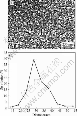
Fig.1(a) presents the SEM image of the typical cobalt doped ZnO nanostructured films prepared by low energy cluster beam deposition. We can clearly observe that the film is assembled by the spherical nanoparticles that are distributed uniformly and monodispersely in the film. The formation of such nanoparticle film is attributed to the unique LECBD preparation process. In detail, during the LECBD process, the phase formation of nanoclusters (or nanoparticles) is achieved in the former condensation chamber at high temperature, while the deposition of cobalt doped ZnO nanocluster beam onto the Si substrate is achieved in the hinder ultrahigh vacuum chamber at low energy and low temperature. Both processes are independent of each other[18]. Consequently, the nanoparticles deposited on the substrate will not inosculate with each other. Thus, the cobalt doped ZnO film will be assembled by nanoparticles. The EDX results confirm that the approximate composition for the nanoparticles is Zn1-xCoxO at x=0.1. Fig.1(b) plots the graph of population versus size distribution of the nanoparticles. It is clear that the size distribution for these monodisperse nanoparticles are narrow, in the range of 25-35 nm. The mean diameter of the nanoparticles is 29.3 nm. Meanwhile, the particle size distribution is almost lognormal. In fact, the growth of the clusters as well as their size distribution is mainly determined by the cluster residence time and its distribution. Under the present Ar gas pressure, the carrier gas flows mainly in the form of convection current and the clusters move to a major extent due to drift. In this case, the residence time distribution is lognormal, which has been proved by KISS et al[19].

Fig.1 SEM image (a) and graph (b) of population versus size distribution of typical as-deposited cobalt doped ZnO film
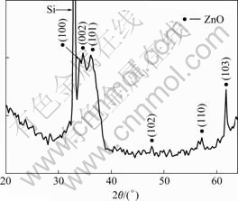
Fig.2 shows the typical XRD pattern of cobalt doped ZnO nanostructured film. The peaks in Fig.2 can be indexed to wurtzite hexagonal ZnO phase with cell constants a=3.248 ? and c=5.206 ? except for the signal of the substrate. And no obvious diffraction peaks of cobalt metallic or compound were detected. The result shows that the film possesses hexagonal wurtzite structure.

Fig.2 XRD pattern of as-deposited film
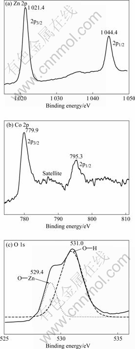
In order to further investigate the chemical bonding states in cobalt doped ZnO film, X-ray photoelectron spectroscopy (XPS) was used to characterize the structure, and the results are shown in Fig.3. The XPS spectra have been corrected to the adventitious C 1s peak at 284.2 eV. One can observe the core state of Zn 2p, and Co 2p. The binding energies of Zn 2p3/2 and Zn 2p1/2 are located at 1 021.4 and 1 044.4 eV, respectively, as illustrated in Fig.3(a). At the same time, the binding energies of Co 2p3/2 and Co 2p1/2 are located at 779.9 and 795.3 eV, respectively, as shown in Fig.3(b). The Co 2p main peaks have a satellite structure, which is on the lower binding-energy side. These results indicate a divalent state of cobalt in the nanostructured film. The O 1s state XPS spectrum is shown in Fig.3(c), in which the curve is split into two peaks. The peak at 529.4 eV can be attributed to the O-Zn bond formation, while the peak at 531.0 eV can be attributed to the formation of O-H bond. The characteristic of XPS spectra shows that cobalt is not simple substance or cluster but divalent state in Co doped ZnO nanostructured film. Hence, divalent Co maybe replaces divalent Zn atom in the formation of Co doped ZnO cluster-assembled nanostructured film.

Fig.3 XPS spectra of Co doped ZnO film: (a) Zn 2p; (b) Co 2p; (c) O 1s
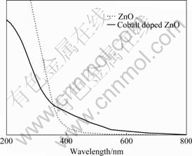
Optical absorption spectrum of cobalt doped ZnO film assembled by nanoparticles is shown in Fig.4. The absorption of pure cluster-assembled ZnO nanostructured film was also measured and is also shown in Fig.4. The optical absorption spectra of the both films have a sharp absorption edge. However, compared with the absorption of pure cluster-assembled ZnO film, the absorption edge of cobalt doped ZnO film exhibit is an obvious blue shift, which shows that the optical band-gap of the film is broadened after doping. These results show that the optical absorption properties vary after doping Co for cluster-assembled ZnO nanostructured film.

Fig.4 Optical absorption spectra of cobalt doped ZnO nanostructured film assembled by nanoparticles and pure cluster-assembled ZnO nanostructured film
4 Conclusions
1) Cobalt doped ZnO nanostructured films assembled by the nanoparticles were prepared by the low energy cluster beam deposition method.
2) The nanostructured film is assembled by uniform and monodispersed spherical nanoparticles.
3) Cobalt doped ZnO nanostructured film is indexed to a wurtzite structure of ZnO and the optical band-gap of the film is broadened after doping.
References
[1] LOOK D C. Recent advances in ZnO materials and devices [J]. Mater Sci Eng B, 2001, 80: 383-387.
[2] RENSMO H, KEIS K, LINDSTROM H, SODERGREN S, SOLBRAND A, HAGFELDT A, LINDQUIST S E, WANG L N, MUHAMMED M. High light-to-energy conversion efficiencies for solar cells based on nanostructured ZnO electrodes [J]. Journal of Physics Chemistry, 1997, 101(14): 2598-2601.
[3] JO S H, LAO J Y, REN Z F, FARRER R A, BAKDACCHINI T, FOURKAS J T. Field-emission studies on thin films of zinc oxide nanowires [J]. Applied Physics Letters, 2003, 83: 4821-4823.
[4] KADOTA M, MINAKATA M. Piezoelectric properties of ZnO films on a sapphire substrate deposited by an RF-magnetron-mode ECR sputtering system [J]. Japanese Journal of Applied Physics, 1998, 37: 2923-2926.
[5] KITTILSTVED K R, NORBERG N S, GAMELIN D R. Chemical manipolation of high-Tc ferromagnetism in ZnO diluted magnetic semiconductors [J]. Physics Review Letters, 2005, 94: 147209.
[6] TSUKAZAKI A, OHOTMO A, ONUMA T, OHTANI M, MAKINO T, SUMIYA M, OHTANI K, CHICHIBU S A, FUKE S, SEGAWA Y, OHNO H, KOINUMA H, KAWASAKI M. Repeated temperature modulation epitaxy for p-type doping and light-emitting diode based on ZnO [J]. Nature Materials, 2005, 4: 42-46.
[7] FUKUMURA T, LIN Z, KAWASAKI M, SHONO T, HASEGAWA T, KOSHIHARA S, KOINUMA H. Magnetic properties of Mn-doped ZnO [J]. Applied Physics Letters, 2001, 78: 958-960.
[8] SHAMA P, GUPTA A, RAO K V, OWENS F J, SHARMA R, AHUJA R, OSORIO J M, GUILLEN O, JOHANSSON B, GEHRING G A. Ferromagnetism above room temperature in bulk and transparent thin films of Mn-doped ZnO [J]. Nature Materials, 2003, 2: 673-677.
[9] LIN Z, FUKUMURA T, KAWASAKI M, ANDO K, SAITO H, SEIGUCHI T, LOO Y Z, MURAKAMI M, MATSUMOTO Y, HASEGAWA T, KOINUMA H. High throughput fabrication of transition-metal-doped epitaxial ZnO thin films: A series of oxide-diluted magnetic semiconductors and their properties [J]. Applied Physics Letters, 2001, 78: 3824-3826.
[10] CHO Y M, CHOO W K, KIM H, KIM D IHM Y E. Effects of rapid thermal annealing on the ferromagnetic properties of sputtered Zn1-x(Co0.5Fe0.5)xO thin films [J]. Applied Physics Letters, 2002, 80: 3358-3360.
[11] CHIKOIDZE E, DUMONT Y, JOMARD F, BALLUTAUD D, GALTIER P, GOROCHOV O, FERRAND D. Semiconducting and magnetic properties of Zn1-xMnxO films grown by metalorganic chemical vapor deposition [J]. Journal of Applied Physics, 2005, 97: 10D327.
[12] PARK J H, KIM M G, JANG H M, RYU S, KIM Y M. Co-metal clustering as the origin of ferromagnetism in Co-doped ZnO thin films [J]. Applied Physics Letters, 2004, 84: 1338-1340.
[13] LEE H J, JEONG S Y, CHO C R, PARK C H. Study of diluted magnetic semiconductor: Co-doped ZnO [J]. Applied Physics Letters, 2002, 81: 4020-4022.
[14] ZHAO S F, YAO M L, WAN J G, MU Y W, ZHOU J F, WANG G H. The microstructure and magnetic behaviour of Co nanostructured film prepared by energetic cluster beam deposition [J]. European Physics Journal D, 2009, 52: 163-166.
[15] SONG F Q, HAN M, LIU J D, CHEN B, WAN J G, WANG G H. Experimental observation of nanojets formed by heating PbO-coated Pb clusters [J]. Physics Review Letters, 2005, 94: 093401
[16] ZHAO S F, BI F, WAN J G, HAN M, SONG F Q, LIU J M, WANG G H. Cluster-assembled Tb-Fe nanostructured films produced by low energy cluster beam deposition [J]. Nanotechnology, 2007, 18: 265705.
[17] ZHAO S F, WU Y J, WAN J G, DONG X W, LIU J M, WANG G H. Giant magnetoelectric effect in Tb-Fe/Pb(Zr0.52Ti0.48)O3 thin-film heterostructure prepared by low energy cluster beam deposition [J]. Applied Physics Letters, 2008, 92: 012920.
[18] BINNS C. Nanoclusters deposition on surface [J]. Surface Science Reports, 2001, 44: 1-49.
[19] SODERLUND J, KISS L B, NIKLASSON G A, GRANQVIST C G. Lognormal size distributions in particle growth processes without coagulation [J]. Physics Review Letters, 1998, 80: 2386-2388.
Foundation item: Projects(10904065; 10674056; 10774070; 90606002) supported by the National Natural Science Foundation of China; Project (20080441042) supported by China Postdoctoral Science Foundation; Project(200926) supported by Tonghua Normal University Foundation; Project(2010CB923401) supported by the National Basic Research Program of China; Project(BK2008024) supported by the Natural Science Foumdation of Jiangsu of Province, China
Corresponding author: ZHAO Shi-feng; Tel: +86-13675171342; E-mail: shfzhao@sina.com
DOI: 10.1016/S1003-6326(09)60049-2
(Edited by YANG Hua)