Trans. Nonferrous Met. Soc. China 22(2012) s148-s152
Determination of trap levels in CZT:In by thermally stimulated current spectroscopy
NAN Rui-hua1, JIE Wan-qi1, ZHA Gang-qiang1, BAI Xu-xu2, WANG Bei3, YU Hui1
1. State Key Laboratory of Solidification Processing, School of Materials Science and Engineering, Northwestern Polytechnical University, Xi’an 710072, China;
2. Key Laboratory of Artificial Structures and Quantum Control, Ministry of Education, Department of Physics, Shanghai Jiao Tong University, Shanghai 200240, China;
3. Science Institute, Air Force Engineering University, Xi’an 710051, China
Received 9 July 2012; accepted 16 August 2012
Abstract: Many defects in semi-insulating (SI) cadmium zinc telluride (Cd1-xZnxTe or CZT) ingots grown by the melt methods act as trapping centers to introduce deep levels in the band gap, which has strong effects on CZT detection properties. The thermally stimulated current (TSC) spectroscopy was used to measure these traps, and the initial rise method and the simultaneous multiple peaks analysis (SIMPA) method were introduced to characterize trap levels in SI-CZT:In. The results show that there is a larger error in the determination for the trap peaks with the initial rise method due to the interference of overlapping peaks, while the SIMPA method demonstrates a better performance in resolving these overlapping peaks simultaneously for a full characterization of trap levels. On this basis, a theoretical SIMPA fitting, which is composed of ten trap levels and a deep donor level EDD dominating the dark current in SI-CZT:In, is achieved. Furthermore, the reason of high resistivity in CZT:In was explained by the relationship between EDD level and Fermi level.
Key words: Cd1-xZnxTe; trapping; deep levels; thermally stimulated current spectroscopy
1 Introduction
Semi-insulating (SI) cadmium zinc telluride (Cd1-xZnxTe or CZT) is an advanced material for fabricating X-ray and gamma-ray detectors operating at room temperature because of its high resistivity and good mobility-lifetime products [1-4]. The high resistivity is obtained by electrical compensation processes: usually, group III (Al, Ga, In) or group VII (Cl) elements are doped to compensate the native defects effectively in the material [5,6]. However, there are different defects in CZT ingots grown by the melt methods, including native defects, residual impurities and complexes, which act as trapping centers to introduce deep levels in the band gap [7,8]. These deep levels exert strong effects on the electrical properties and charge transport behaviors, determining the final detector performance properties [9,10]. Therefore, the identification and characterization of the electrically active defects are of considerable importance for controlling and improving CZT detection properties.
Defects in SI-CZT crystals can be characterized by thermally stimulated current (TSC) spectroscopy. In TSC measurement, the energy level of a particular trap is related to the temperature at which it is emptied, while the number of traps contributing to the stimulated peak is obtained from the amount of charge release. Actually, the precise determination of trap levels in CZT material by TSC measurement is difficult due to the mutual interference of overlapping peaks and their poor resolutions [11,12]. In previous studies, PAVLOVIC and DESNICA [13] have proved an assumption that the measured TSC spectra in CdZnTe material were composed of many overlapping peaks. The initial rise and the SIMPA methods were introduced to comparatively resolve TSC spectra for a full characterization of trap levels which affect charge transport behaviors of indium-doped Cd1-xZnxTe (x=0.1) detector. As a consequence, an effective analysis method was determined for an accurate evaluation of trap levels in SI-CZT material.
2 Experimental
SI-Cd1-xZnxTe:In (x=0.1) crystal with the indium content of 1×10⁻⁵ was grown by the modified vertical Bridgman (MVB) method in our laboratory, which was described in detail [14,15]. Wafer in the size of 10 mm×5 mm×1 mm cut from the ingot was etched in 2% bromine methanol solution to remove the damaged surface layer, and then electroless Au contacts were deposited with AuCl3 solution. The electrical resistivity of the crystal was measured to be about 100 GΩ・cm at room temperature by an Agilent 4155C semiconductor parameter analyzer.
In TSC measurement, the wafer was placed in a closed-cycle cryostat with liquid helium (Sumitomo DE- 202 closed-cycle refrigerator) and cooled in darkness to 25 K, where the deep traps were filled using a halogen lamp. Then, as the traps were emptied by thermal emission in darkness until 310 K at heating rate of 0.25 K/s with bias voltage of 10 V, TSC currents as a function of temperature were obtained by a Keithley 6514 electrometer. During the experiments, the wafer was kept in darkness to prevent the excitation of charge carriers by light, avoiding unintentional deep trap filling. In the meantime, the temperature dependence of dark current (IDC) was determined by performing the above described procedures without illumination at low temperature.
In addition, the temperature-dependent resistivity was investigated by current-voltage measurement with planar contacts in the range from 271 K to 321 K with bias voltages from -10 V to 10 V.
3 Results and discussion
3.1 Initial rise method
The initial rise method, a kind of “thermal cleaning” procedure, is based on the assumption that the traps begin to empty as the temperature increases [16]. A whole TSC curve from 25 K to 310 K in a SI-CZT:In sample is obtained where the heating rate was 0.25 K/s with bias voltage of 10 V in Fig. 1 (the dashed curve), the sample was subsequently re-cooled down to 25 K and then irradiated again. When it was measured through the same cycle once more, the heating was stopped at a temperature T between T1 and T2. In this way, the traps responsible for the current peaks for T2 were substantially emptied and thus the resulting TSC currents were obtained. After subtracting the impact of the dark current, the isolated TSC peak at the temperature of T1 was obtained. Then, the sample was re-cooled and re-heated in darkness in the temperature range from T2 to T3 so as to obtain the isolated T2 peak. Finally, the results of this procedure are illustrated in Fig. 1, where the solid curves are the isolated TSC currents for the corresponding temperature intervals defined above. By isolating the whole TSC curve with the initial rise method, five main trap peaks are observed, namely T1, T2, T3, T4 and T5 at the energy level of 0.091, 0.151, 0.202, 0.337 and 0.436 eV, respectively. It is clearly shown that only parts of the isolated trap peaks with the initial rise method are similar to the results of the whole measured TSC curve, such as the traps of T1 and T4, while others (like the traps of T2, T3 and T5) are apart from the whole measured TSC result or even isolated multi-peaks. This indicates that the TSC curve from CZT:In is not a classical single spectrum but complex. During the thermal emission procedure of TSC measurement, the simultaneous release of charge carriers from different traps may lead to the neighboring traps overlapping and thus cause the additional shifts of maximum peak in the whole measured TSC curve. The existence of overlapping peaks with poor resolutions and inevitable interference may bring a larger error to the isolation of trap peaks with the initial rise method. As a result, the simultaneous isolation of overlapping peaks in a complex TSC spectrum is very important for characterizing trap levels to the full.
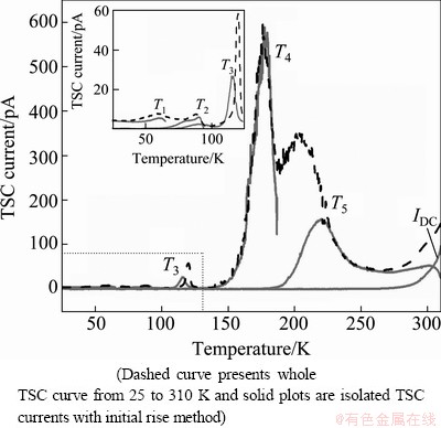
Fig. 1 TSC spectra from SI-CZT:In sample and isolation of trap peaks with initial rise method
3.2 Simultaneous multiple peak analysis (SIMPA) method
In order to determine all trap levels simultaneously and decrease the sum of offset errors to a minimum from the TSC spectrum with overlapping peaks in SI-CZT:In, the SIMPA method reported by PAVLOVIC and DESNICA [13] is introduced.
The temperature dependence of fitting function, ISIMPA, comprising the sum of TSC peaks belonging to the specific deep levels ITSC and the dark current IDC, is defined by
 (1)
(1)
where  is the ith individual TSC peak; m is the number of deep traps involved in calculation;
  , C is a constant, k is the Boltzmann’s constant, and EDD is the deep donor activation energy which dominates the dark current.
In the first order kinetics approximation, a single TSC peak resulting from an electron trap can be described as

 (2)
(2)
where e is the electron charge, u is the carrier mobility, τ is the carrier lifetime, A is the area of electrode, E is the applied electric field, T is the absolute temperature, β is the heating rate, m0 is the rest mass, m is the effective mass, Ea,i is the thermal activation energy of the ith trap which is related to the TSC peak position, and σi is the capture cross section of the ith trap.
In addition, NT,i represents the carrier concentration of the i-th trap at the beginning of the temperature ramp, which can be calculated from
 (3)
(3)
where  denotes the temporal integral of
 , that is
 . Therefore, the trap signatures concentration (NT), thermal activation energy (Ea) and capture cross section (σ) of deep levels in SI-CZT:In can be obtained by above calculations.
This method clearly indicates where TSC peaks are “missing” and/or overlapping. Figure 2 presents the SIMPA fit of the TSC curve obtained from the SI-CZT:In. The dashed curve denotes the whole TSC spectra as mentioned above and the solid curves correspond to each individual TSC peak defined by Eqs. (1) and (2) which belongs to a specific trap. As a result, a better fit is achieved by a theoretical function, which is composed of ten trap levels and the EDD level dominating the dark current. By calculation with the SIMPA method, the trap signatures of observed traps are characterized simultaneously and the results are presented in Table 1. In comparison with the initial rise method, the SIMPA fit demonstrates very good performance in resolving the composition of overlapping peaks simultaneously to the individual trap peaks and therefore results in the evaluation of real trap values.
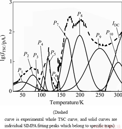
Fig. 2 TSC spectra on SI-CZT:In with SIMPA method
Table 1 Trap signatures of observed trap levels in SI-CZT:In determined with SIMPA method
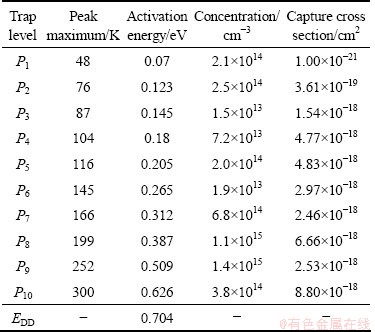
Among these traps, trap P1, with an activation energy of 0.07 eV, a capture cross section of 1.00×10⁻²¹ cm2 and a concentration of 2.1×1014 cm-3, is deduced as an acceptor level. The defect associated with this level is probably correlated with the impurity (Au, Ag, etc) [17]. Traps with similar activation energies are also often identified as the acceptor level of Cd vacancy [18].
Trap P2 with Ea, σ and NT of 0.123 eV, 3.61×10⁻¹⁹ cm2, 2.5×1014 cm-3, respectively, and trap P3 (0.145 eV, 1.54×10⁻¹⁸ cm2, 1.5×1013 cm-3) may correspond to the shallow acceptor level (or band) of the so-called A center, which is reported in the range of 0.12-0.15 eV [19]. The microscopic origin of this level has been attributed to (VCd-InCd) complex.
Trap P4 (0.18 eV, 4.77×10⁻¹⁸ cm2, 7.2×1013 cm-3) and trap P5 (0.205 eV, 4.83×10⁻¹⁸ cm2, 2.0×1014 cm-3) may be assigned to the electron levels of TeCd+ or the TeCd related defects [10,20], which correspond to the level at 0.20 eV in Ref. [10] and the TEES defect P0 or P1 in Ref. [20].
Trap P6 (0.265 eV, 2.97×10⁻¹⁸ cm2,1.9×1013 cm-3) is at the same position as the peak of level C found in Cd0.9Zn0.1Te by CAVALLINI et al [21]. The origin of this level is probably attributed to the structural defects introduced by compositional segregation, precipitation, inclusion and/or constitutional super-cooling.
Trap P7 (0.312 eV, 2.46×10⁻¹⁸ cm2, 6.8×1014 cm-3) corresponding to the trap T3 at 0.321 eV confirmed by an inductively coupled plasma mass spectroscopy (ICP-MS) analysis in Ref. [12] may be ascribed to the acceptor level formed by impurity Cu.
Trap P8 (0.387 eV, 6.66×10⁻¹⁸ cm2, 1.1×1015 cm-3) is similar to the level at 0.4 eV reported by BERDING [22], which is assigned to an electron trap from the doubly ionized tellurium antisite (TeCd2+) related defects or complexes.
Trap P9 with Ea of 0.509 eV may be attributed to Cd vacancy (VCd) above the valence band. EMANUELSSON et al [23] also observed this level by photo-electron paramagnetic resonance (Photo-EPR) measurement (0.47 eV), which corresponds to the acceptor level of double ionized Cd vacancy.
Trap P10 (0.626 eV, 8.80×10⁻¹⁸ cm2, 3.8×1014 cm-3) may be claimed to have an acceptor character and Zn-related origin. The defects at 0.55-0.65 eV associated with Zn cation vacancy have been found in PICTS measurements of Cd0.9Zn0.1Te and Cd0.8Zn0.2Te [19, 24].
Furthermore, the deep donor level EDD dominates the dark current above room temperature in SI-CZT:In, which is similar to the ‘EL2’ mid-gap level in SI-GaAs [25]. By calculation, the EDD level at 0.704 eV near the mid-gap of CZT:In at room temperature (Eg=1.57 eV) is determined. It is generally accepted that high resistivity CZT materials are achieved through the pinning of the Fermi level EF near mid-gap by compensation. The EDD level plays an important role in compensation precesses, and it is responsible for the Fermi level pinning near the mid-gap [26]. To further confirm the hypothesis, the Fermi level of the SI-CZT : In by the linear fit of temperature dependence of resistivity was calculated, ln ρ∝ΔE/(kT) [27], as shown in Fig. 3. By fitting the plots of ln ρ―1/(kT), the Fermi level in SI-CZT:In is determined to be (0.740±0.047) eV.
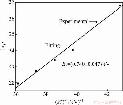
Fig. 3 Fermi level by fitting plots of ln ρ versus (kT)-1
4 Conclusions
1) There is a larger error in evaluating the values of deep traps with the initial rise method, which is caused by the interference of overlapping peaks.
2) The SIMPA method demonstrates a better performance in isolating the composition of overlapping peaks simultaneously to the individual trap peaks and thus to obtain more reliable values of trap levels.
3) Based on the SIMPA fit, ten trap levels and a deep donor level EDD dominating the dark current in SI-CZT:In and their origins are identified. At the same time, the high resistivity of CZT:In is explained to be responsible for the Fermi level pinning near the mid-gap.
References
[1] SCHLESI NGER T E, TONEY J E, YOON H, LEE E Y, BRUNETT B A, FRANKS L, JAMES R B. Cadmium zinc telluride and its use as a nuclear radiation [J]. Mater Sci Eng R, 2001, 32: 103-189.
[2] BOLOTNIKOV A E, BABALOLA S, CAMARDA G S, CUI Y, GUL R, EGARIEVWE S U, FOCHUK P M, FUERSTNAU M, HORACE J, HOSSAIN A, JONES F, KIM K H, KOPACH O V, MCCALL B, MARCHINI L, RAGHOTHAMACHAR B, TAGGART R, YANG G, XU L, JAMES R B. Correlations between crystal defects and performance of CdZnTe detectors [J]. IEEE Trans Nucl Sci, 2011, 58(4): 1972-1980.
[3] STEFANO D S, ABBENE L, CAROLI E, MANCINI A M, ZAPPETTINI A, UBERTINI P. Progress in the development of CdTe and CdZnTe semiconductor radiation detectors for astrophysical and medical applications [J]. Sensors, 2009, 9: 3491- 3526.
[4] LI Xia, CHU Jun-hao, LI Long-xia, DAI Ning, SUN Jing-lan, ZHANG fu-jia. Development of room temperature CdZnTe nuclear radiation detector [J]. Semiconductor Technology, 2008, 133(11): 941-946.
[5] FRABONI B, CAVALCOLI D, CAVALLINI A, FOCHUK P. Electrical activity of deep traps in high resistivity CdTe: Spectroscopic characterization [J]. J Appl Phys, 2009, 105(7): 073705.
[6] LI Gang, SANG Wen-bin, MIN Jia-hua, QIAN Yong-biao, SHI Zhu-bin, DAI Lin-gen, ZHAO Yue. Study on the defect energy levels of high resistivity In-doped CdZnTe crystals [J]. Journal of Inorganic Materials, 2008, 23(5): 1049-1053.
[7] GUL R, BOLOTNIKOV A, KIM H K, RODRIGUEZ R, KEETER K, LI Z, GU G, JAMES R B. Point defects in CdZnTe crystals grown by different techniques [J]. J Electron Mater, 2011, 40(3): 274- 279.
[8] GUL R, KEETER K, RODRIGUEZ R, BOLOTNIKOV A E, HOSSAIN A, CAMARDA G S, KIM K H, YANG G, CUI Y, CARCELEN V, FRANC J, LI Z, JAMES R B. Point defects in Pb-, Bi-, and In-doped CdZnTe detectors: Deep-level transient spectroscopy (DLTS) measurements [J]. J Electron Mater, 2012, 41(3): 488-493.
[9] CAVALLINI A, FRABONI B, DUSI W, ZANARINI M, SIFFERT P. Deep levels and compensation in gamma-irradiated CdZnTe [J]. Appl Phys Lett, 2000, 77(20): 3212-3214.
[10] CARVALHO A, TAGANTSEV A K, OBERG S, BRIDDON P R, SETTER N. Cation-site intrinsic defects in Zn-doped CdTe [J]. Phys Rev B, 2010, 81(7): 075215.
[11] PAVLOVIC M, JAKSIC M, ZORC H, MEDUNIC Z. Identification of deep trap levels from thermally stimulated current spectra of semi-insulating CdZnTe detector material [J]. J Appl Phys, 2008, 104(2): 023525.
[12] NAN Rui-hua, JIE Wan-qi, ZHA Gang-qiang,WANG Tao, XU Ya-dong, LIU Wei-hua. Investigation on defect levels in CdZnTe:Al using thermally stimulated current spectroscopy [J]. J Phys D Appl Phys, 2010, 43(34): 345104.
[13] PAVLOVIC M, DESNICA U V. Precise determination of deep trap signatures and their relative and absolute concentrations in semi-insulating GaAs [J]. J Appl Phys, 1998, 84(4): 2018-2022.
[14] LI Guo-qiang, ZHANG Xiao-lu, HUA Hui, JIE Wan-qi. A modified vertical Bridgman method for growth of high-quality Cd1-xZnxTe crystals [J]. J Electron Mater, 2005, 34(9): 1215-1224.
[15] LI Guo-qiang, JIE Wan-qi, GU Zhi, YANG Ge, WANG Tao. CdZnTe energy levels Induced by doping of indium [J]. Chin Phys Lett, 2004, 21(2): 367-369.
[16] MICOCCI G, RIZZO A, TEPORE A. Trapping center parameters in indium selenide single crystals by thermally stimulated current measurements [J]. J Appl Phys, 1983, 54(4): 1924-1929.
[17] SZELES C. Advances in the crystal growth and device fabrication technology of CdZnTe room temperature radiation detectors [J]. IEEE Trans Nucl Sci, 2004, 51: 1242-1249.
[18] CHU M, TERTERIAN S, TING D, WANG C C, GURGENIAN H K, MESROPIAN S. Tellurium antisites in CdZnTe [J]. Appl Phys Lett, 2001, 79(17): 2728-2730.
[19] CASTALDINI A, CAVALLINI A, FRABONI B, FERNANDEZ P, PIQUERAS J. Deep energy levels in CdTe and CdZnTe [J]. J Appl Phys, 1998, 83: 2121-2126.
[20] ELHADIDY H, FRANC J, BELAS E, HLIDEK P, MORAVEC P, GRILL R, HOSCHL P. Thermoelectric effect spectroscopy and photoluminescence of high-resistivity CdTe:In [J]. J Electron Mater, 2008, 37(9): 1219-1224.
[21] CAVALLINI A, FRABONI B, DUSI W, ZANAEINI M. Defective states induced in CdTe and CdZnTe detectors by high and low energy neutron irradiation [J]. J Appl Phys, 2003, 94(5): 3135- 3142.
[22] BERDING M A. Native defects in CdTe [J]. Phys Rev B, 1999, 60: 8943-8950.
[23] EMANUELSSON P, OMLING P, MEYER B, WIENECKE M, SCHENK M. Identification of the cadmium vacancy in CdTe by electron paramagnetic resonance [J]. Phys Rev B, 1993, 47(23): 15578-15580.
[24] CASTALDINI A, CAVALLINI A, FRABONI B, POLENTA L, FERNANDEZ P, PIQUERAS J. Cathodoluminescence and photoinduced current spectroscopy studies of defects in Cd0.8Zn- 0.2Te [J]. Phys Rev B, 1996-I, 54(11): 7622-7625.
[25] KABIRAJ D, GHOSH S. EL2-related metastable defects in semi-insulating GaAs [J]. Appl Phys Lett, 2004, 84(10): 1713-1715.
[26] KUBAT J, ELHADIDY H, FRANC J, GRILL R, BELAS E, HOSCHL P, PRAUS P. Evaluation of the concentration of deep levels in semi-insulating CdTe by photoconductivity and TEES [J]. IEEE Trans Nucl Sci, 2009, 56(4): 1706-1711.
[27] XU Ya-dong, JIE Wan-qi, SELLIN P, WANG Tao, LIU Wei-hua, ZHA Gang-qiang, VEERAMANI P, MILLS C. Study on temperature dependent resistivity of indium-doped cadmium zinc telluride [J]. J Phys D Appl Phys, 2009, 42(3): 035105.
热激电流谱确定CZT:In中的陷阱能级
南瑞华1,介万奇1,查钢强1,白旭旭2,王 蓓3,于 晖1
1. 西北工业大学 材料科学与工程学院学院 凝固技术国家重点实验室,西安 710072;
2. 上海交通大学 物理系 人工结构及量子调控教育部重点实验室,上海 200240;
3. 空军工程大学 理学院,西安 710051
摘 要:熔体法生长的半绝缘碲锌镉(Cd1-xZnxTe或者CZT)晶体中存在着很多缺陷,这些缺陷作为陷获中心在带隙中引入了深能级,从而严重影响CZT的探测性能。分别采用初始上升法和同步多峰分析法(SIMPA)分析热激电流谱(TSC),从而获得了半绝缘的铟掺杂的Cd0.9Zn0.1Te晶体中的陷阱能级分布。结果表明:由于重叠峰的干扰,初始上升法在确定陷阱峰的最大值时会产生较大的误差;而SIMPA法被证实适用于分离重叠峰,可同步获得较全面的陷阱能级分布。基于此,获得了半绝缘CZT:In晶体的缺陷能级分布结果,即包含十个陷阱能级和一个影响暗电流分布的深施主能级EDD。此外,通过EDD能级与费米能级的关系,解释了CZT:In晶体获得高阻特性的原因。
关键词:Cd1-xZnxTe;陷获;深能级;热激电流谱
(Edited by LI Yan-hong)
Foundation item: Projects (61274081, 50902113, 50902114) supported by the National Natural Science Foundation of China; Project (2011CB610406) supported by the National Basic Research Program of China; Project (B08040) supported by the 111 Project of China; Project (JC20100228) supported by Foundation for Fundamental Research of Northwestern Polytechnical University (NPU), China; Project (SKLSP201012) supported by the Research Fund of the State Key Laboratory of Solidification Processing (NPU), China
Corresponding author: NAN Rui-hua; Tel: +86-29-88493135; Fax: +86-29-88495414; E-mail: ruihuanan@gmail.com

