
Microstructure evolution of AZ91D induced by high energy shot peening
HOU Li-feng(侯利锋)1, 2, WEI Ying-hui(卫英慧)1, 2, LIU Bao-sheng(刘宝胜)2, XU Bing-she(许并社)1, 2
1. College of Materials Science and Engineering, Taiyuan University of Technology, Taiyuan 030024, China;
2. Key Laboratory of Interface Science and Engineering in Advanced Materials, Ministry of Education,
Taiyuan University of Technology, Taiyuan 030024, China
Received 12 December 2007; accepted 7 May 2008
Abstract: A nanostructured surface layer was fabricated on a AZ91D magnesium alloy by using a high-energy shot peening(HESP). HESP induced structure along the depth of the treated sample surface layer was characterized by means of X-ray diffractometer (XRD), transmission electron microscope(TEM) and high resolution transmission electron microscope(HRTEM). The experimental results show that a deformed layer of about 50 μm has formed after HESP treatment and the average grain size increases from about 40 nm in the surface layer to about 200 nm at the depth of 40 μm. The surface nanocrystallization can realize intercoordination of the dislocations slipping and dynamic recrystallization. The nanocrystalline grains have stacking faults and dislocation in their interiors. The microhardness of the top surface is about triplicate that of the coarse-grained matrix.
Key words: AZ91D magnesium alloy; high-energy shot peening(HESP); nanocrystalline
1 Introduction
Nanocrystallization by severe plastic deformation (SPD) in metal materials has been a subject of many researches[1-3] in the last decade. This method offers two significant advantages compared with other techniques such as high-energy ball milling, insert gas condensation. First, it is possible to produce large bulk samples. Second, these samples are free from any residual porosity and contamination. Among those methods, high energy shot peening(HESP) is one of the effective processings for the fabrication of various ultrafine-grained structures by imposing intense plastic strains onto the surface of the metals and alloys. The strains present gradient distribution in the surface layer, changing from the maximum at the top surface to near zero far into the matrix. The microstructure observation at various depth levels can, therefore, provide the clue to the process of structural evolution relevant to various stages of strain.
So far, the ultrafine-grain or nanocrystalline has been fabricated in several metal materials such as aluminum and its alloys[4-5], low carbon steel[6-8], stainless steel[9-11], titanium[12], cobalt[13-14], iron [15] and copper[16]. Most documented experimental and theoretical investigations have shown that the grain refinement is originated from dislocation activities during deformation in cubic (face-centered cubic(FCC) and body-centered cubic(BCC) as well) metals and alloys with a medium or high stacking fault energy(SFE). By contrast, the low SFE FCC materials exhibit a different mode of grain refinement, which involves the slip of dislocation and subsequent deformation twinning, followed by interplay of twins with dislocations. As for the hexagonal close packed(HCP) metals, deformation twinning occurs at the early stage of deformation and severs as an additional deformation mechanism to dislocation slip[13]. These results illustrate the refinement mechanism of the investigated metals. However, more metals should be examined to extend the application of the HESP.
The characteristic properties of magnesium alloys, like density, high specific strength/stiffness, good damping capacity, diecastability and recycling potential make them ideal candidates to replace heavier materials (steel, aluminum) in automotive industry to meet the mass reduction demand. This has drawn attention of more and more materials researchers. The widely used magnesium alloys belong to Mg-Al-Zn(AZ) series, such as AZ91(Mg-9Al-1Zn), showing excellent castability, good room temperature mechanical properties and low cost. AZ91D magnesium alloy has a medium SFE (50-80 mJ/m2), consists of α-phase (Mg matrix) and β-phase (Mg17Al12). To understand the mechanism of plastic deformation and improve the mechanical properties, an understanding of the origin and mechanism of grain refinement during HESP has intrinsic merit. In the present study, we investigated the microstructure change in the various layer of AZ91D magnesium alloy subjected to HESP treatment through TEM and HRTEM, with the aim at establishing the mechanism of grain refinement and strain accommodation during HESP, providing insight into optimal methods for grain refinement and the improvement of mechanical properties.
2 Experimental
The AZ91D alloy used in the present investigation was a plate of 5 mm in thickness with chemical composition (mass fraction, %) of 8.63 Al, 0.66 Zn, 0.29 Mn and balance Mg. The alloy plate was cut into pieces with a dimension of 100 mm×100 mm suitable to HESP processing. A smooth surface was attained by polishing on 700-grade SiC paper. Microscope examination revealed an initial grain size of about 120 μm. The apparatus used in this study was the same as that reported in Ref.[4]. During HESP process, the hardened stainless steel balls of 6 mm in diameter were placed at the bottom of a vacuum chamber attached to a vibration generator. Because of the high vibration frequency of the system, the sample surface to be treated was impacted respectively by a large number of balls within a short period of time. Each impacting resulted in plastic deformation in the surface layer of the treated sample. As a consequence surface, nanocrystallization was conducted on the sample. In this work, the treatment was performed for 7.5 min and 30 min, respectively, at room temperature with a vibrating frequency of 50 Hz under vacuum.
The X-ray diffraction analysis was carried out on a Rigaku D/MAX2400 X-ray diffractometer, with Cu Kα radiation. The microstructures in the given depth from the surface to the matrix of the sample were observed by H-800 transmission electron microscope(TEM) and JEOL-2010 high resolution transmission electron microscope(HRTEM). The sample for TEM observation was finally thinned by ion-milling. The cross-section microhardness measurement was conducted along the depth from the surface of the sample by MVK-H3 Vickers hardness meter.
3 Experimental results
3.1 Microstructures
The XRD patterns of AZ91D magnesium alloys before and after HESP treatments are shown in Fig.1. After HESP treatment, there is broadening of the Bragg reflection profiles, which may be attributed to grain refinement and the microstrain development.
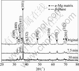
Fig.1 XRD patterns of AZ91D magnesium alloys with HESP for various times
The deformed layer is about 50 μm thick subjected to HESP treatment for 30 min, observed by means of optical microscope. Based on the experimental results, the increase of HESP treatment duration does not change the grain size of the surface layer, but increases the thickness of the nanocrystalline layer[17].
The microstructure of the sample after HESP treatment for 30 min was also observed. Fig.2 shows a TEM image of the layer in a depth of about 60 μm from the surface layer of sample. A great number of dislocations tangling(DT) and dislocation wall(DW) are formed inside the grains. Therefore, the inhomogenously distributed dislocations result in the formation of high dislocation density area and low dislocation density area, which is the initial stage of the subgrain.
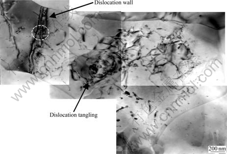
Fig.2 TEM image showing dislocation walls and dislocation tanglings marked by black arrows (about 60 μm in depth) in AZ91D alloy after HESP for 30 min
The TEM micrograph (Fig.3) shows the grain size of 200 nm at an increased strain (about 40 μm deep below treated surface). The contrast is different among grains, indicating the existence of high internal stresses. Also there are many “clean” grains as shown in the figure with the arrow. These are the typical characteristic of dynamic recrystallization.
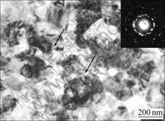
Fig.3 Bright field image and corresponding SAED pattern of refined grains of about 40 μm in depth
Fig.4 shows a TEM micrograph illustrating theequiaxed microstructure in the nanometer region. The image is taken at the outer surface of the layer (about 10 μm deep from the top surface). The average grain size is determined to be 40 nm. The corresponding SAED pattern is also presented. The ring-like electron diffraction pattern shows that grain orientation is random, indicating highly misoriented boundaries.

Fig.4 TEM micrographs of surface layer (about 10 μm thickness) of sample after HESP for 30 min: (a) Bright-field image; (b) Dark-field image showing equiaxed nanograins; (c) Corresponding SAED pattern
Fig.5 shows a HRTEM micrograph of the layer in a depth of about 10 μm from the top surface of sample after HESP treatment for 30 min. This shows that the grains orientate randomly and are characterized by high angle grain boundary. This further proves that the subgrains with low angle boundary evolve into nanocrystalline with high angle boundary with an increase in strain and disordered orientation of the grain increases. In particular, these grains have stacking faults (indicated by arrowheads) and dislocation (shown in circle) in their interior even at initial stage of formation.
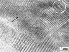
Fig.5 HRTEM micrograph of nanocrystalline
The above-mentioned results show that the microstructures change from subgrains far from the top surface layer to grains of about 200 nm with high angle grain boundaries and to grains about 40 nm near the top surface layer. This indicates that with the increase of the strain, deformation undergoes the changes from dislocations tangling and microsubgrain to ultrafine- grains finally. As the strain increases, the subgrains near the original grain boundary start to evolve into high angle grain boundary.
3.2 Hardness variation
Fig.6 shows the microhardness variation along the depth from the treated surface of the sample after HESP for 30 min. In the top surface nanostructured layer, the microhardness is enhanced. Compared with that of the matrix of sample, the microhardness of the top surface nanocrystalline layer is about triplicate that of the coarse-grained matrix, and the hardness of the layer of 40 μm below the surface is increased too. With the further increase in depth, the hardness variation tends to be steady. The increase of the surface hardness of the sample after HESP treatment is attributed to the coactions of the grain refinement and the work-hardening. So it can be concluded that the surface nanocrystalline is helpful to the surface strengthening of materials.
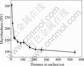
Fig.6 Hardness variation of sample after HESP for 30 min with distance from topmost to substrate
4 Discussion
Based on the TEM observations, the grain refinement will be discussed in terms of strain accommodation at different levels of strain. At the low strain level during the HESP process, the imposed strain is accommodated mainly by dislocation slipping in the matrix with HCP structure, as shown in Fig.2, rather than by deformation twinning as often found in HCP materials.
The grain boundaries are reported to act as obstacles for slip and dislocation. The nucleation should happen especially in certain deformation inhomogeneities like grain boundaries and triple junction, as shown in Fig.3. This phenomenon may be understood in terms of dynamic recrystallization(DRX) mechanism. In HESP process, high strains may be induced into the deformed metals, thus create some highly strained regions, such as grain boundaries and triple junctions. These areas may store enough energy to allow nucleation of small subgrains to occur. With high levels of dislocation density, small energy fluctuation resulted from impacts during the HESP process can trigger DRX. In addition, the temperature in the treated layer will rise due to repetitive peening of balls during HESP process and hence, the onset of DRX is easy to happen. The subgrain boundaries are of unequilibrium and consist of large dislocation nets, causing the formation of the internal strain. Simultaneously, the misorientations of subgrains increase with strain and evolve into high angle boundary though the dislocation regrouping. The process of grain subdivision may proceed successively to finer scale with strain, resulting in the formation of ultrafine crystallines and nanocrystallines. Hence, the refinement mechanism of AZ91D magnesium alloy induced by HESP treatment is the co-actions of two mechanisms, i.e. dislocations slipping and DRX operation simultaneously. The schematic illustration of refinement mechanism is shown in Fig.7.
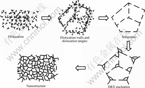
Fig.7 Schematic illustration showing microstructural evolution process of AZ91D magnesium alloy induced by HESP
5 Conclusions
1) The nanocrystalline layer is successfully fabricated on the surface of the AZ91D magnesium alloy by high-energy shot peening(HESP). The nanocrystalline grains are of about 40 nm size and have stacking faults and dislocation in their interior.
2) The grain refinement mechanism of AZ91D magnesium alloy induced by HESP treatment is the co-operation of dislocation slipping and DRX operation simultaneously.
3) Mechanical property measurement indicates a significant increment of hardness in the surface layer with nanostructures subjected to HESP treatment. Compared with that of the matrix of sample, the microhardness of the top surface is about triplicate that of the coarse-grained matrix.
References
[1] KORZNIKOV A V, IVANISENKO YU V, LAPTIONOK D V, SAFAROV I M, PILYUGIN V P, VALIV R Z. Influence of severe plastic deformation on structure and phase composition of carbon steel [J]. Nanostructured Materials, 1994, 4(6): 159-167.
[2] TAO N R, SUI M L, KU J, KU L. Surface nanocrystallization of iron induced by ultrasonic shot peening [J]. Nanostructured Materials, 1999, 11(4): 433-557.
[3] SHIN D H, KIM B C, KIM Y S, PARK K T. Microstructural evolution in a commercial low carbon steel by equal channel angular pressing [J]. Acta Materialia, 2000, 48(9): 2247-2255.
[4] HU Lan-qing, WANG Ke, LIU Gang, XU Bing-she. Microstructure characteristics of as-surface nanocrystallized 1420 aluminum alloy by high-energy shot peening [J]. Trans Nonferrous Met Soc China, 2005, 15(3): 615-617.
[5] WU X, TAO N, HONG Y, XU B, LU J, LU K. Microstructure and evolution of mechanically-induced ultrafine grain in surface layer of Al-alloy subjected to USSP [J]. Acta Materialia, 2002, 50(8): 2075-2084.
[6] YONG Xing-ping, LIU Gang, L? Jian, LU Ke. Surface nanocrystallization of low carbon steel [J]. Acta Metallurgica Sinica, 2002, 38(2): 157-160. (in Chinese)
[7] WANG Z B, LU J, LU K. Chromizing behaviors of a low carbon steel processed by means of surface mechanical attrition treatment [J]. Acta Materialia, 2005, 53(7): 2081-2089.
[8] LIU G, WANG S C, LOU X F, LU J, LU K. Low carbon steel with nanostructured surface layer induced by high-energy shot peening [J]. Scripta Materialia, 2001, 44(8/9): 1791-1795.
[9] LIU G, LU J, LU K. Surface nanocrystallization of 316L stainless steel induced by ultrasonic shot peening [J]. Mater Sci Eng A, 2000, 286(2): 91-95.
[10] ZHANG H W, HEI Z K, LIU G, LU J, LU K. Formation of nanostructured surface layer on AISI 304 stainless steel by means of surface mechanical attrition treatment [J]. Acta Materialia, 2003, 51(7): 1871-1881.
[11] CHEN X H, LU J, LU L, LU K. Tensile properties of a nanocrystalline 316L austenitic stainless steel [J]. Scripta Materialia, 2005, 52(10): 1039-1046.
[12] ZHU K Y, VASSEL A, BRISSET F. Nanostructure formation mechanism of α-titanium using SMAT [J]. Acta Materialia, 2004, 52(14): 4101-4110.
[13] WU X, TAO N, HONG Y, LU J, LU K. γ→ε martensite transformation and twinning deformation in FCC cobalt during surface mechanical attrition treatment [J]. Scripta Materialia, 2005, 52(7): 547-551.
[14] WU X, TAO N, HONG Y. Strain-induced grain refinement of cobalt during surface mechanical attrition treatment [J]. Acta Materialia, 2005, 53(2): 681-691.
[15] TAO N R, WANG Z B, TONG W P, SUI M L, LU J, LU K. An investigation of surface nanocrystallization mechanism in Fe induced by surface mechanical attrition treatment [J]. Acta Materialia, 2002, 50(18): 4603-4616.
[16] WANG K, TAO N R, LIU G, LU J, LU K. Plastic strain-induced grain refinement at the nanometer scale in copper [J]. Acta Materialia, 2006, 54(12): 5281-5291.
[17] WEI Ying-hui, LIU Bao-sheng, HOU Li-feng, XU Bing-she, LIU Gang. Characterization and properties of nanocrystalline surface layer in Mg alloy induced by surface mechanism attrition treatment [J]. Journal of Alloys and Compounds, 2008, 452(2): 336-342.
Foundation item: Projects(50471070, 50644041) supported by the National Natural Science Foundation of China; Project(20041023) supported by Youth Science and Technology Foundation of Shanxi Province, China; Project(200503005) supported by Key Laboratory Opening Foundation of Shanxi Province, China
Corresponding author: HOU Li-feng; Tel: +86-351-6018685; E-mail: houlifeng78@126.com
(Edited by YANG Bing)