Theoretical and experimental investigation on giant magnetoresistive materials with amorphous ferromagnetic layer
WEN Qi-ye(���ҵ), ZHANG Huai-wu(�Ż���), SONG Yuan-qiang(��Զǿ), JIANG Xiang-dong(����)
School of Microelectronic and Solid-state Electronic,
University of Electronic Science and Technology of China, Chengdu 610054, China
Received 10 April 2006; accepted 25 April 2006
Abstract: Pseudo-spin-valve (PSV) sandwiches using amorphous CoNbZr alloy as soft magnetic layer were fabricated by magnetron sputtering. The giant magnetoresistance (GMR) and its dependence on the thickness of magnetic layer were investigated. Anti-parallel magnetization alignments were observed in the samples with very thin CoNbZr thickness (2-4 nm) and a maximum GMR ratio of 6.5% was obtained. The Camley-Barnas semiclassical model was extended for amorphous layer based magnetic sandwiches by considering that the mixed layers exist between the ferromagnetic and nonmagnetic layer. The calculated results agree with the experimental results very well, indicating that the new model gives a more realistic picture of the physical processes that take place in the magnetic sandwiches. Moreover, the calculated results for amorphous sandwiches also clarify that the occurrence of maximum GMR at very small thickness of amorphous layer is ascribed to the short mean-free-path in amorphous materials.
Key words: giant magnetoresistance; pseudo-spin-valve; amorphous ferromagnetic layer; Camley-Barnas model
1 Introduction
Pseudo-spin-valve (PSV) sandwiches using very thin amorphous film as soft layer have been reported to exhibit a relatively large giant magnetoresistance (GMR) of 4%-6% in low field [1-4]. The very small thickness (��10 nm) is a great advantage for reducing both the size and the demagnetizing effect of GMR devices with small feature such as GMR head and magnetic random access memory cell [5]. Though quite a few types of amorphous soft layer such as CoFeB [1, 2], CoMnB [3] and CoNbZr [5-7] have been studied as the soft layer of PSV and magnetic tunnel junction, the effects of these amorphous layer on the quality of the trilayers, especially the interfacial microstructure, have not been investigated so far, and no theoretical model are proposed to address this amorphous structure.
In this paper, PSVs with structure of CoNbZr/Co/Cu/Co were studied. The Camley-Barnas model [8-10] was extended to magnetic sandwiches by assuming mixed layers exist between the ferromagnetic and nonmagnetic layers. The calculation can reproduce the experimental results very well, indicating that the new model gives a more realistic picture of the physical processes that take place in the magnetic sandwiches.
2 Experimental and discussion
CoNbZr/Co(1 nm thick)/Cu(2.2 nm thick)/Co(4 nm thick) were prepared by DC magnetron sputtering on natural oxidized Si(100) substrates without any buffer layers. The thickness of CoNbZr layer, dCNZ, varies from 1 to 10 nm. The Cu and Co targets are 99.95% pure metal while the composition of the CoNbZr targets is Co85.5Nb9Zr5.5 (atom fraction, %). The base pressure of the deposit system is 13 ��Pa and the sputtering Ar pressure is 26 mPa. The sputtering rates of CoNbZr, Cu, and Co were 0.16, 0.20, and 0.25 nm/s, respectively. All samples were capped with a 5 nm thick Ta layer. The GMR ratio was measured using a four-probe technique with 1 mA orthogonal current and magnetic field in the film plane. The hysteresis loops of the films were measured by alternating gradient magnetometers at room temperature.
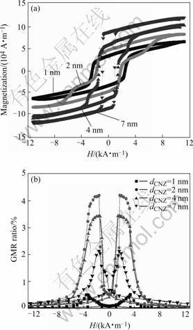
Fig.1 shows the typical hysteresis loop and MR curves of CoNbZr/Co/Cu/Co PSV. As to the sample with 1 nm-thick CoNbZr layer, no obvious plateau was observed in the hystemesis loop. The very small MR ratio of 0.5% may result from the anisotropic magnetoresistance of the Co layer. The samples with 2 and 4 nm thick CoNbZr layer (hereafter denoted as samples 2 and 4, respectively) show obvious two-stage magnetization process and relatively large GMR ratios, which indicates the different effective coercivities and independent magnetization reversals of CoNbZr and Co layer. Samples 2 and 4 show larger GMR ratio of 4.5% and sharper magnetization reversal process for both Co and CoNbZr layers with a field sensitivity above 16.6%?m?kA-1.

Fig.1 Typical hysteresis loops (a) and GMR curves (b) of CoNbZr/Co/Cu/Co PSV
The two-stage magnetization process vanishes and the MR ratio decreases to below 1% when dCNZ is increases to 10 nm, suggesting that the magnetization reversal of both layers occurs nearly simultaneously. Of course, the shunting effect and the short electronic mean-free-path of amorphous CoNbZr also contribute to the significant drop of MR when dCNZ increases to 10 nm. As it can be seen from Fig.1 (a), the switching field of the amorphous soft layer, Hws, increases with the decrease of thickness. The Hws is about 800 A/m for sample with 10 nm-thick CoNbZr layer but increases beyond 2 400 A/m for sample wtih 1 nm thick CoNbZr layer. Surprisingly, the switching field of the top Co layer has a more significant increase with the decrease of the thickness of CoNbZr layer though the thickness is identical for all samples. The switching field of Co layer is 800 A/m when dCNZ =10 nm. However, this value increases sharply to 2 800 A/m for dCNZ =4 nm and about 5 600 A/m for dCNZ= 2 nm.
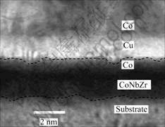
One possible interpretation for the dCNZ dependence of the switching field is that the microstructures, and consequently the magnetostatic coupling, are different in samples with different thickness of CoNbZr layer. In order to clarify this problem, the cross-sections of PSVs with 2 nm thick CoNbZr layer, as a demonstration, were investigated using HRTEM. The TEM image is shown in Fig.2. It is clearly seen that the substrate has a rough surface with root-mean-square larger than 0.5 nm, and the interfaces of the Cu layer look wavy. The interfacial atomic mix regions at the bottom and top surfaces of Cu layer are clear observed, which is estimated to be 0.2-0.5 nm.

Fig.2 TEM image of CoNbZr(2 nm)/Co/Cu/Co
3 Theoretical model
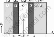
Above experimental results shows that samples with very thin ferromagnetic layer (2-4 nm) exhibit large GMR ratio, and interfacial atomic mix regions exist at the ferromagnetic (FM) layer and non-magnetic(NM) layer interfaces, which may have a significant affection on the GMR effect. Therefore, we consider the spin-valve structure as illustrated in Fig.3. Two FM layers are separated by a NM layer, and with thin mixed regions (Mix) between the FM and NM layer. The Mix layer can be seen as a part of the FM layer that contains a certain amount of NM atoms. Therefore the following aspects were assumed.
1) Mix layer has the same magnetization direction as its neighboring FM layer.
2) The mean-free-path(MFP) of the spin up/down electrons in this mixed region is smaller than that in FM layer since it is structurally amorphous, but the spin-asymmetry-scattering factor (Nb) is assumed to be the same for simplification.
3) The scattering at the outer boundaries of the sandwich is purely diffusive since there is no evidence to support the specular scattering in a magnetic sandwich.
According to the Camley-Barnas model, the boltzmann equation in each region only depends on the coordinate z. When applying an electric field Ex along the x axis, the boltzmann equation in the relaxation-time

Fig.3 Schematic diagram of spin-valve with two mixed layer
approximation are written as:
 (1)
(1)
where e is the electron charge, �� is the spin-dependent relaxation time, m is the electron effective mass in each region, v is the electron velocity, f0 is the equilibrium distribution function and gis is the corrected term in region i for spin s. The gis in each layer is divided into two parts: one for electrons with positive vz, gi+s, and another one for negative vz, gi-s. The general solutions for gis in the region A can be written as
 (2)
(2)
The solutions in regions B, D and E have similar forms. In region C, the corrected distribution function is assumed to be Z independence thus has the form:
 (3)
(3)
Parameters A��s, B��s, C��s and D��s are determined by the boundary conditions described as
 (4)
(4)
 (5)
(5)
 (6)
(6)
 (7)
(7)
 (8)
(8)
 (9)
(9)
where T(?) and R(?) are the transmission and reflection coefficients of electrons with spin up (down) at the interfaces. �� is the angle between the magnetization of the FM layers. At the outer boundaries the conditions have the forms:
 (10)
(10)
 (11)
(11)
where p is the specular scattering factor which together with R is assume to be zero in following calculations. A general expression of the current density along the X axis can be given as:
 (12)
(12)
With Eqn.(12) the effective conductivity can be obtained as s��J/2bEx. Hence the GMR is defined by
��s/s0=(s0-s��)/s0 (13)
where s0��s��-0.
In the appropriate calculations, the product of resistvity and MFP, �Ѧ�, can be assumed to be a constant. This assumption works well for simple metals and it is also usually applied for transition metals, though in the later case there are deviations from this approximation. For amorphous CoNbZr film, the previous study shows that after crystallization its resistivity decreases from 1.5 to 0.5 ��cm. This means that �� of the amorphous CoNbZr is approximately three times smaller than that of the crystallined one. At the same time, since the percentage of Nb and Zr are low, the properties of the crystallized CoNbZr are close to that of Co. Therefore, the average electron MFP of FM layers, ��FM,av=(��FM��+��FM��)/2, was chose to be 2.5, 1.5, and 1.0 nm respectively. The MFP of Mix layer was set to be half of ��FM,av and the electron MFP in NM layer, ��Cu, was fixed to 20 nm in all cases since it is rather larger than the thickness of NM layer. According to above experiments, dMix=0.25 nm was used in the calculation. The interface spin-asymmetry-
scattering factor (Ns) of Mix/NM was assumed to be 10 with T��=0.92 and T��=0.20.
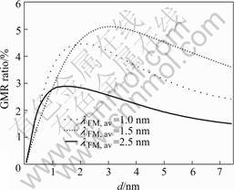
Fig.4 shows the calculated GMR ratios of CoNbZr/Cu/CoNbZr sandwiches with various ��FM,av. the GMR increases as FM thickness increasing, then start to decrease after achieving the maximum value. This feature confirms the experimental observation mentioned above. Furthermore, both the maximum GMR ratio and corresponding FM thinkness d decrease with the decrease of ��. The maximum GMR ratio and d are 12% and 3.5 nm for ��FM,av=7 nm while 6.4% and 1.8 nm for ��FM,av=3 nm.

Fig.4 Calculated results of GMR ratio vs thickness of CoNbZr in CoNbZr/Cu/CoNbZr trilayers with Ns=10, dMix=0.25 nm, dCu=2 nm, ��Co=2��Mix, and ��Cu=20 nm
As we can see, when dCNZ��d, the results derived from ��FM,av=1.5 nm fit the experimental values quite well. The maximum GMR ratio of 4.45% was figured out to be at dFM =2.1 nm, which also agrees with the experimental value. However, when the nominal thickness of CoNbZr is 1 nm, the experimental maximum GMR is less than 0.5%, which is much smaller than the calculated value. One possible reason is that a continuous CoNbZr with thinckness of 1 nm is hard to be formed so a ��spin-valve�� effect cannot be well realized. Interestingly, the calculations show that smaller MFP gives rise to larger GMR ratio when FM layer is very thin. This suggests that a thin FM layer could provide sufficient spin-dependent-scattering to the spin electrons with small MFP, while to the electrons with larger MFP a thin FM layer is not enough. This result unambiguously explains that the small FM thinkness of amorphous sandwiched structure ascribes to the very
short MFP of amorphous magnetic system.
4 Conclusion
In this work, PSVs using amorphous CoNbZr alloy as soft magnetic layer were fabricated by magnetron sputtering. Anti-parallel magnetization alignments were observed in the samples with very thin CoNbZr thickness (2-4 nm) and a maximum GMR ratio of 6.5% was obtained. The Camley-Barnas semiclassical model was extended for amorphous layer based magnetic sandwiches by considering that mixed layers exist between the ferromagnetic and nonmagnetic layer. The calculated results agree with the experimental results very well, and clarify that the occurrence of maximum GMR at very small thickness of amorphous layer is ascribed to the short mean-free-path in amorphous materials.
Reference
[1] JIMBO M, KOMIYAMA K, TSUNASHIMA S. Giant magnetoresistance effect and electric conduction in amorphous-CoFeB/Cu/Co sandwiches[J]. J Appl Phys, 1996, 79(8): 6237-6239.
[2] JIMBO M, KOMIYAMA K, SHIROTA Y. Thermal stability of spin valve using amorphous CoFeB[J]. J Magn Magn Mater, 1997, 165: 308-311.
[3] SAKAKIMA H, SATOMI M, IRIE Y, KWWAWAKE Y. Magnetoresistance in CoMnB/Co(Fe)/Cu/Co(Fe) spin valves[J]. J Magn Magn Mater, 1997, 165: 108-110.
[4] DAUGHTON J M. GMR and SDT sensor applications[J]. IEEE Trans Magn, 2000, 36: 2773-2778.
[5] KIM J S, KIM Y K��LEE S R. Thermal and Mn diffusion behaviors of CoNbZr-based spin valves with nano oxide layers, 2003, 39(5): 2824�C2826.
[6] WEN Q Y, ZHANG H W, JIANG X D, SHI Y, TANG X L, ZHANG W L, HAN B S, MAGN J. Enhancement of the magnetoresistance in rapid recurrent thermal annealed Co/Cu/Co/CoNbZr spin value multilayers[J]. J Magn Magn Mate, 2004, 282(1-3): 100-104.
[7] PARK S J, PARK W J, KIM Y J, KIM T W. Magnetic tunnel junctions with low Ms free layers[J]. Physica Status Solidi A: Applied Research, 2004, 201(8): 1640�C1643.
[8] CAMLEY R E, BARNAS J. Theory of giant magnetoresistance effects in magnetic layered structures with antiferromagnetic coupling[J]. Phys Rev Lett, 1989, 63(6): 664�C667.
[9] XU M, WANG Y, LUO G M. Dependence of giant magnetoresistance on the thickness of magnetic and non-magnetic layers in spin-valve sandwiches[J]. Phys Lett A, 2000, 272(4): 282�C288.
[10] XU M, WANG Y, LIU C X, MAI Z H. Effect of inserting a ferromagnetic layer on the giant magnetoresistance of spin-valve sandwiches[J]. J Appl Phys, 2003, 93(1): 325�C329.
(Edited by ZHAO Jun)
Foundation item: Project (90306015) supported by NSFC; Project supported by Youth Foundation of Science and Technology of UESTC
Corresponding author: Wen Qi-ye; Tel: +86-28-83201810; Fax: +86-28-83201810; E-mail: qywen@163.com