
J. Cent. South Univ. (2019) 26: 2943-2952
DOI: https://doi.org/10.1007/s11771-019-4226-0

Inverse Stone-Thrower-Wales defect and transport properties of 9AGNR double-gate graphene nanoribbon FETs
Mohammad Bagher NASROLLAHNEJAD, Parviz KESHAVARZI
Electrical and Computer Engineering Department, Semnan University, Semnan, Iran
 Central South University Press and Springer-Verlag GmbH Germany, part of Springer Nature 2019
Abstract: Defect-based engineering of carbon nanostructures is becoming an important and powerful method to modify the electron transport properties in graphene nanoribbon FETs. In this paper, the impact of the position and symmetry of the ISTW defect on the performance of low dimensional 9AGNR double-gate graphene nanoribbon FET (DG-GNRFET) is investigated. Analyzing the transmission spectra, density of states and current-voltage characteristics shows that the defect effect on the electron transport is considerably varied depending on the positions and the orientations (the symmetric and asymmetric configuration) of the ISTW defect in the channel length. Based on the results, the asymmetric ISTW defect leads to a more controllability of the gate voltages over drain current, and drain current increases more than 5 times. The results have also confirmed the ISTW defect engineering potential on controlling the channel electrical current of DG-AGNR FET.
Key words: inverse Stone-Thrower-Wales defect; electronic transport properties; graphene nanoribbon; tight binding; NEGF formalism
Cite this article as: Mohammad Bagher NASROLLAHNEJAD, Parviz KESHAVARZI. Inverse Stone-Thrower-Wales defect and transport properties of 9AGNR double-gate graphene nanoribbon FETs [J]. Journal of Central South University, 2019, 26(11): 2943-2952. DOI: https://doi.org/10.1007/s11771-019-4226-0.
1 Introduction
Graphene is a 2D semi-metallic nanomaterial arranged in honeycomb lattice structure [1, 2]. This material has many unique properties, including superior thermal and electrical conductivity [3, 4] as well as extremely high carrier mobility at room temperature [5, 6]. However, the lack of intrinsic bandgap in graphene causes some impediments for its electronic digital applications [7]. The lack of bandgap creates very low on/off current ratios in graphene transistors and consequently these devices cannot be switched off and it causes a major disadvantage in electronic digital applications.
Several methods have been proposed to increase the intrinsic bandgap in graphene lattices, such as forming graphene nanoribbons via ion beam lithography [8], applying strain [9], and biasing bilayer graphene [10]. Despite the undesirable properties of defects, these imperfections can also lead to some interesting physical and electrical properties of graphene structures [11-16]. There are various types of structural defects in graphene sheets, such as Stone-Wales (SW), adatoms, vacancies and inverse Stone-Thrower-Wales (ISTW) defect which has recently been developed [11].
The simplest type of these in graphene structures is vacancy and adatom defects that result from omitting and adding atoms to the graphene structures, respectively. However, in the SW defect, no carbon is added or omitted and only four hexagons are converted into two heptagons and two pentagons (see Figure 1).
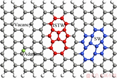
Figure 1 Different type of defects
ISTW is a topological defect that LUSK [17, 18] predicted its structure as a defect on graphene layers. The ISTW structure is similar to SW, but ISTW has two joined 5-membered carbon rings instead of two joined 7-membered carbon rings (see Figure 2) [17-23]. LUSK et al [17, 18] predicted an ISTW defect in graphene structures and investigated the impact of introducing this defect on some important properties such as formation energy, electrostatic potential and electron density.
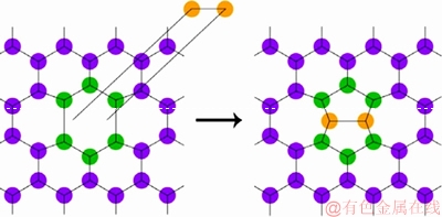
Figure 2 Inverse Stone-Thrower-Wales defect (The left figure shows the initial structure and right figure shows graphene layer after the defect addition)
ISTW defect was recently developed and reported [24-27], but electronic characteristics of graphene with the other defect structures have been extensively investigated [28-37]; therefore there are few investigations regarding ISTW defect [17, 18, 38, 39]. FOTOOHI et al [38, 39] studied transport properties of armchair and zigzag GNR as a two-terminal structure in the presence of ISTW defect. Their results for the two terminal graphene system containing one and two ISTW defects shows that the currents are 5% and 13% less than current calculated of the conventional structure at bias voltage of 0.5 V.
In this paper, we investigated the effect of introducing the ISTW defect in the channel length and in the presence of a complete structure of a low dimensional graphene transistor. It is found that the electronic characteristics of DG-AGNRFET with ISTW defects are distinctively influenced by the symmetry and position of ISTW defect in the channel length. Changing of symmetry and position of the AGNR structures leads to significant modifications in I-V curves.
The rest of this work is organized as follows: Section 2 explains the structure of DG-AGNRFET and computational procedures used in simulations; Section 3 discusses simulation results for the proposed structure. It also indicates how ISTW defects affect the controlling of electron transport in GNR FETs. Finally, Section 4 discusses the important results out of this paper.
2 Device configuration and computational method
We investigate the low dimensional DG-AGNR-FET [40] shown in Figure 3. AGNR is used as a channel material, while the left and right contacts are made from the extensions of the graphene channel. The channel material is composed of 2.556 nm length, N=9 armchair-edge GNR which is placed between the top and bottom dielectric layers with the relative dielectric permittivity 24 and the oxide thickness tins=0.4 nm. All the computations required for the quantum transport were performed using the Slater-Koster tight binding method implemented in quantum wise Atomistix Toolkit (ATK). It has used fully self-consistent tight binding model which is combined with nonequilibrium Green function formalism (NEGF) [41-43].
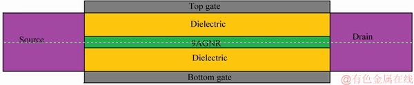
Figure 3 Schematic diagram of DG-AGNR-FET device
The retarded Green��s function (GD) is computed as follows:
 (1)
(1)
where ��s and ��d are the self-energies matrices of source and drain, respectively; HT is the tight-binding Hamiltonian matrix of GNR channel; �� is an infinitesimally small quantity and U is the electrostatic potential obtained using solution of a 3D Poisson equation. Transmission probability can be expressed as:
 (2)
(2)
where ��s/d=i(��s/d-��s/d+) is the energy level broadening of source (drain) contacts; GDa and Gsr represent the advanced (retarded) Green��s function.
The electrical current is calculated using Landauer- Butiker equation [42]:
 (3)
(3)
where T(E) is a probability of passing of electron with energy E through the channel; f(E-��D) is the Fermi-Dirac distribution of carriers in the contacts, ��D is chemical potential in the source and drain contacts; h is the Planck constant and q is the electron charge. The detail of simulation procedure and model equations can be found in Refs. [16, 44, 45]. These structures have been relaxed using the fast pair-potential calculations so that the atomic forces did not exceed 0.001 eV/ and during simulations at 300 K. The Tersoff potential is applied to modeling the atomic interactions. The edge atoms are saturated with hydrogen. The gate bias is 0.5 V in our simulations.
3 Results and discussion
In this paper, a low dimensional DG-AGNR- FET was considered with an ISTW defect in two orientations and three different positions in the channel length. Figure 4 shows atomic structure and transmission pathways [46] of defectless and defective structure with an symmetric and asymmetric ISTW defect. The transmission pathway is a type of analysis map which splits the transmission coefficient into local bond contributions [46]. The contributions can be negative or positive. A negative contribution corresponds to the electron back scattering along the bond. The thickness of each arrow shows the magnitude of the local transmission between each pair of atoms; the arrow and the color determine the direction of the electron current.
In Figure 4(d), it can be seen that when the symmetric ISTW defect is present in the channel region, the transmission pathway is discontinued near the defective region (circled by the red lines). Consequently, the transmission of carriers is strongly confined inside the channel region and the transmission coefficient is decreased. However, the discontinuity of carrier pathway is not too severe in comparison with asymmetric ISTW defective structure (see Figure 4(f)).
Defect leads to localized states at transport direction. Indeed, a series of quantum dots are formed in the GNR channel, in which charges can easily become trapped. Accordingly, electrons can tunnel with applying an external bias and a Coulomb blockade is formed [47]. This phenomenon reveals induction of a transmission gap [48, 49], which is not similar to a true bandgap within 1D graphene regions.
Figure 5 shows the transmission spectrum for defective (symmetric and asymmetric) and defectless DG-AGNR-FET.
Results show that the transmission gaps of defectless, symmetric and asymmetric defective structure are unchanged on 0.8 eV. As depicted in Figure 5, for defectless structure, the first transmission flat part extended to 1 eV above the Fermi level. However, for device with an asymmetric ISTW defect, a wide transmission valley can be seen at 0.76 eV in which the carrier transport is decreased because of intense carrier back-scattering [36]. This is due to carriers localization around the specific atoms marked A and B in Figure 4. Without the influence of backscattering, graphene can exhibit ballistic transport at room temperature, where charge carriers can travel up to ��m-scale distances without scattering [50]. Additionally, the transmission coefficient is also significantly decreased in comparison with conventional structure. These results also confirm the previous simulation results shown in Figure 4.
The current-voltage (I-V) characteristic of the DG-AGNR FET is shown in Figure 6. The current values at the applied bias -1 V in the devices with defectless, symmetric and asymmetric ISTW defective structure are 1.1, 0.8 and 3.96 ��A, respectively.
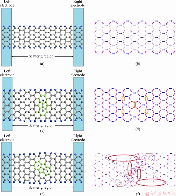
Figure 4 Atomic structure and transmission pathways of defectless (a, b) and defective 9AGNR with an ISTW defect in symmetric (c, d) and asymmetric orientation (e, f) (The gray and blue colored atoms show carbon and hydrogen atoms, respectively. The ISTW defects are highlighted by green atoms)
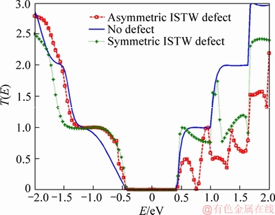
Figure 5 Transmission spectrum for defective (symmetric and asymmetric ISTW defect) and defectless DG-AGNR FET
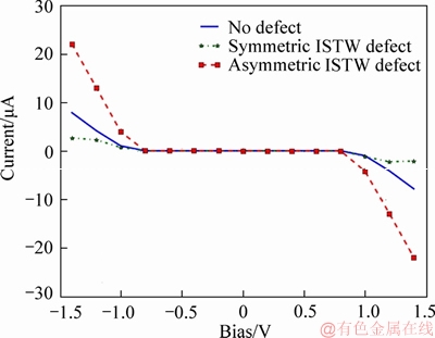
Figure 6 Current-voltage characteristics of defectless and defective DG-AGNR-FET consisting of symmetric and asymmetric ISTW defect (The bias voltage is increased in step of 0.2 V)
The current value in the device with asymmetric ISTW defect (at the applied bias -1 V) is 3.6 times larger than the defectless device��s current. The transport properties of the defective structure greatly depend on both of bandgap narrowing and carrier backscattering. As shown in Figure 6, in spite of decreasing the backscattering, electrical current increases due to narrowing of the bandgap in structure with asymmetric defect [36]. However, the current value in the device with symmetric ISTW defect is less than the current calculated for the defectless structure. Moreover, drain current is decreased in device with symmetric ISTW defect when voltage biases are larger than 1.2 V. The similar current decrease was also seen in the previous effort related to the study of the transport characteristics of AGNR with symmetric ISTW defect [38]. The drain current versus drain�Csource voltage (output characteristics) is also plotted in Figure 7, for VDS from -1.4 to 1.4 V and VGS=0, 0.5 and 1 V. It can be seen that the drain current dependency to the gate voltage for the device with asymmetric ISTW defect is more than that of the defectless device. For the defectless and the asymmetric defective structure, drain current increases as gate voltage increases. But it is vice versa for the symmetric ISTW defective structure. Thus, the asymmetric ISTW defect improves the controllability of the drain current with the gate voltage.
The location of ISTW defect also affects the electronic transport characteristics of GNRFETs.
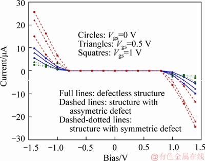
Figure 7 ID�CVDS characteristics of defectless and defective DG-AGNR-FET consisting of symmetric and asymmetric ISTW defect at VGS=0, 0.5 and 1 V
Here, we considered the effect of positions of ISTW defect on device density of states (DOS) and I-V characteristics. Figure 8 shows proposed nanostructures with the left and right symmetric ISTW defect (defect in center position has been shown in Figure 4). Figure 9 shows the DOS characteristics for the defectless and defective structures consisting of the symmetric ISTW defect in three different positions. DOS profile of the device with ISTW defect shows some peaks at the energy levels coincident to localized states caused by ISTW defect [38]. Figure 9 also shows that changing the defect position along the channel length changes the position of the peaks in DOS characteristics. Size of each peak is consistent with the trap densities created by ISTW localized about a particular energy level. On the other hand, the higher the peak, the weaker the coupling between the channel region and the contacts is. In Figure 9, there is a big peak, close to E=0, appearing only when the defect is in the middle of the structure. This peak disappears when the defect is shifted to the left or the right side of the device.
Figure 10 depicts current-voltage characteristics of the simulated device. An asymmetric behavior is observed in positive and negative Vds with different rectification areas (term previously used by KVASHNIN et al [51] for describing the region with zero current). The rectification areas values for defectless and defective structure with the right, the left and the center position of the symmetric ISTW defect are about 1.6 V (in the range from -0.8 to 0.8 V), 1.8 V (in the range from -0.8 to 1 V), 1.8 V (in the range from -1 to 0.8 V) and 1.6 V (in the range from -0.8 to 0.8 V), respectively. As shown, changing the position of the ISTW defect in the vicinity of the source or drain leads to an increase of 12.5% of rectification area. Therefore, I-V characteristics show a sort of asymmetry behavior in the presence of the left and the right symmetric ISTW defects.
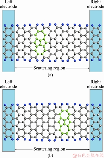
Figure 8 Schematics of AGNR with left symmetric ISTW defect (a) and right symmetric ISTW defect (b)
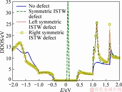
Figure 9 Device density of states (DDOS) characteristics of defectless and defective AGNRs with symmetric ISTW defect in three different positions
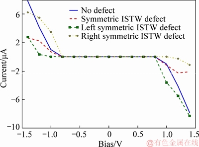
Figure 10 Current-voltage characteristics of defectless and defective AGNRs with symmetric ISTW defect in three different positions
The drain current at the applied bias -1 V in the defectless and defective structures with the right, the left, and the center position of the symmetric ISTW defect is 1.1, 3.58, 0.07 and 0.8 ��A, respectively. The drain current in the device with right symmetric ISTW defect (at the applied bias -1 V) is 3.25 times larger than drain current of defectless device. As a result, if the symmetric ISTW defect is located in left side of the channel, the drain current increases in positive biases and if it is located in right side, the drain current increases in negative voltage biases.
There is a perfect correspondence between the I(V) curve for the symmetric defect located on the left part of the ribbon, and the -I(-V) curve for the symmetric defect located on the right part.
Figure 11 shows the DOS characteristics for the defectless and defective AGNRs consisting of asymmetric ISTW defect in three different positions (in the same positions of the symmetric ISTW defect in Figure 8). It is observed that the presence of the asymmetric ISTW defect leads to creating some peaks in DOS characteristics that is larger than peaks of DOS in the symmetric ISTW defective device. Figure 11 also shows that changing the location of the defects across the channel leads to changing the position of the peaks in DOS characteristics.
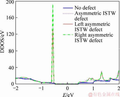
Figure 11 Device density of states (DDOS) characteristics of defectless and defective AGNRs with asymmetric ISTW defect in three different positions
Figure 12 shows current-voltage characteristics of simulated structure with asymmetric ISTW defect at three different positions. The results show that rectification area for defective and defectless device is about unchanged. The current values at the applied bias -1 V in the devices with the right, the left, the center position of the asymmetric ISTW defect and defectless structure are 2.02, 5.63, 3.96 and 1.1 ��A, respectively. Thus the device with left asymmetric ISTW defect (at the applied bias -1 V) achieves an ON-current that its value is 5 times bigger than that in a defectless device. Accordingly, we can increase electrical current by creating an asymmetric ISTW defect in the left side of the channel length and symmetric ISTW defect in the right side of the channel length. The similar increase of the electrical current was also observed in the previous effort devoted to the study of the electronic transport properties of AGNR with symmetric and asymmetric SW defect [36]. But the current value for device with symmetric SW defect was greater than the value of that in asymmetric SW defective device. While, this is vice versa for the ISTW defected devices. Moreover, in the positive bias voltages, drain current of ��device with asymmetric ISTW defect in the right side of the channel�� is greater than the drain current of ��the device with the left side defect��. But this is vice versa for the negative bias voltages. Thus device with ISTW defect is sensitive to current direction. As a general result, the asymmetric ISTW defect increases the drain current in all three channel positions for any biases. But symmetric ISTW defect only increases the drain current when bias is positive and defect is in the left side of the channel length or when bias is negative and defect is in the right side.
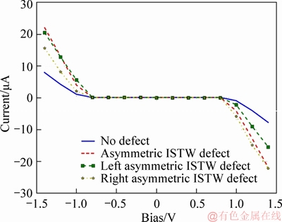
Figure 12 Current-voltage characteristics of defectless and defective AGNRs with asymmetric ISTW defect in three different positions
Figure 13(a) shows the drain current versus the gate voltage for defectless and defective structure with the symmetric and asymmetric ISTW defect (both center positions). In Figure 13(a), at Vg=0.3 V, there is a sudden decrease of the drain current by a factor of 3. This curve shows a negative differential resistance. This behavior has been observed in different graphene structures with different physical origins [52-59]. Figure 13(b) shows this I-VGS characteristics for the defectless and ISTW defective structures with the asymmetric defect at three different (right, center and left) positions. It indicates that the asymmetric ISTW defect increases the drain current for all three defect positions.
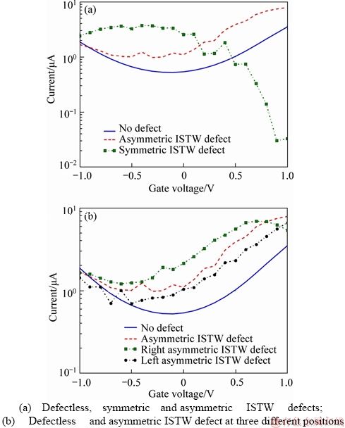
Figure 13 I-VGS characteristics of defectless and defective AGNRs:
Our results have indicated that electronic transport characteristics of the GNRFETs can be significantly influenced by structural defect. Moreover, the position and orientation of this defect also have an important effect on the controlling electronic transport of GNRFETs.
4 Conclusions
This paper presents a theoretical investigation on low dimensional defective DG-AGNR-FET to study of ISTW defect engineering. It is found that the position and orientation of ISTW defects can effectively alter the transport properties of the DG-AGNR-FETs. Our simulations results have indicated that ISTW defect can increase the drain current up to 5 times compared to the conventional structure. Furthermore, changing the position of symmetric ISTW defect in the vicinity of the source or drain can lead to an asymmetry behavior. Simulations indicated that the asymmetric ISTW defect always increases the drain current, while the symmetric ISTW defect increases the drain current in a shorter range of biases. Moreover the asymmetric ISTW defect improves the controllability of the drain current with the gate voltage and the ION also increases for the device with defect in the left and center position of the channel length. Simulation results have implied the possibility of tuning the transport properties in the DG-AGNR FETs using ISTW defect engineering that is useful for enhancing GNR based nanodevice performance.
References
[1] GEIM A K, NOVOSELOV K S. The rise of graphene [J]. Nat Mater, 2007, 6: 183-191.
[2] HE Y, LIU Y G. Direct fabrication of highly porous graphene/TiO2 composite nanofibers by electrospinning for photocatalytic application [J]. Journal of Central South University, 2018, 25(9): 2182-2189.
[3] BALANDIN A A, GHOSH S, BAO W, CALIZO I, TEWELDEBRHAN D, MIAO F, LAU C N. Superior thermal conductivity of single-layer graphene [J]. Nano Lett, 2008, 8: 902-907.
[4] WU Z T, HU F Y, ZHANG Y, GAO Q, CHEN Z P. Mechanical analysis of double-layered circular graphene sheets as building material embedded in an elastic medium [J]. Journal of Central South University, 2017, 24(11): 2717-2724.
[5] CHEN J H, JANG C, XIAO S, ISHIGAMI M, FUHRER M S. Intrinsic and extrinsic performance limits of graphene devices on SiO2 [J]. Nat Nanotechnol, 2008, 3: 206-209.
[6] HAQUE A M, KWON S, KIM J, NOH J, HUH S, CHUNG H, JEONG H. An experimental study on thermal characteristics of nanofluid with graphene and multi-wall carbon nanotubes [J]. Journal of Central South University, 2015, 22(8): 3202-3210.
[7] SCHWIERZ F. Graphene transistors: Status, prospects, and problems [J]. Proc IEEE, 2013, 101: 1567-1584.
[8] HUANG C H, SU C Y, OKADA T, LI L J, HO K I, LI P W, CHEN I H, CHOU C, LAI C S, SAMUKAWA S. Ultra-low-edge-defect graphene nanoribbons patterned by neutral beam [J]. Carbon, 2013, 61: 229-235.
[9] NI Z H, YU T, LU Y H, WANG Y Y, FENG Y P, SHEN Z X. Uniaxial strain on graphene: Raman spectroscopy study and band-gap opening [J]. ACS Nano, 2008, 2: 2301-2305.
[10] ZHANG Y, TANG T T, GIRIT C, HAO Z, MARTIN M C, ZETTL A, CROMMIE M F, SHEN Y R, WANG F. Direct observation of a widely tunable bandgap in bilayer graphene [J]. Nature, 2009, 459: 820-823.
[11] TERRONES M, BOTELLO-M NDEZ A R, CAMPOS- DELGADO J, L
 PEZ-UR
 AS F, VEGA-CANT
 Y I, RODRGUEZ-MACAS F J, ELAS A L, MUNOZ- SANDOVAL E, CANO-M
 RQUEZ A G, CHARLIER J C, TERRONES H. Graphene and graphite nanoribbons: Morphology, properties, synthesis, defects and applications [J]. Nano Today, 2010, 5: 351-372.
[12] CARR L D, LUSK M T. Defect engineering: Graphene gets designer defects [J] Nat Nanotechnol, 2010, 5: 316-317.
[13] XU H, ZHANG D, CHEN L. Effect of defect on electronic properties of zigzag graphene nanoribbons [J]. Journal of Central South University (Science and Technology), 2012, 43(9): 3510-3516. (in Chinese)
[14] BANHART F, KOTAKOSKI J, KRASHENINNIKOV A V. Structural defects in graphene [J]. ACS Nano, 2011, 5: 26-41.
[15] VICARELLI L, HEEREMA S J, DEKKER C, ZANDBERGEN H W. Controlling defects in graphene for optimizing the electrical properties of graphene nanodevices [J]. ACS Nano, 2015, 9: 3428-3435.
[16] OWLIA H, KESHAVARZI P. Locally defect-engineered graphene nanoribbon field-effect transistor [J]. IEEE Trans Electron Dev, 2016, 63: 3769-3775.
[17] LUSK M T, WU D T, CARR L D. Graphene nanoengineering and the inverse Stone-Thrower-Wales defect [J]. Phys Rev B, 2010, 81: 155444.
[18] LUSK M T, CARR L D. Nanoengineering defect structures on graphene, [J]. Phys Rev Lett, 2008, 100: 175503.
[19] ORLIKOWSKI D, NARDELLI M B, BERNHOLC J, ROLAND C. Ad-dimers on strained carbon nanotubes: A new route for quantum dot formation [J]. Phys Rev Lett, 1999, 83: 4132-4135.
[20] SGOUROS A, SIGALAS M M, PAPAGELIS K, KALOSAKAS G. Transforming graphene nanoribbons into nanotubes by use of point defects [J]. J Phys Condens Matt, 2014, 26: 125301.
[21] APPELHANS D J, CARR L D, LUSK M T. Embedded ribbons of graphene allotropes: An extended defect perspective [J]. New J Phys, 2010, 12: 125006.
[22] LUSK M T, CARR L D. Creation of graphene allotropes using patterned defects [J]. Carbon, 2009, 47: 2226-2232.
[23] VALENCIA F, ROMERO A H, JESCHKE H O, GARCIA M E. Large-amplitude coherent phonons and inverse Stone-Wales transitions in graphitic systems with defects interacting with ultrashort laser pulses [J]. Phys Rev B, 2006, 74: 075409.
[24] RAMASSE Q M, KEPAPSTOGLOU, D M, HAGE F S, SUSI T, KOTAKOSKI J, MANGLER C, ZAN R. Atom- by-atom STEM investigation of defect engineering in graphene [J]. Micros Microanal, 2014, 20: 1736-1737.
[25] LEHTINEN O, VATS N, ALGARA-SILLER G, KNYRIM P, KAISER U. Implantation and atomic-scale investigation of self-interstitials in graphene [J]. Nano Lett, 2015, 15: 235-241.
[26] ZAN R, RAMASSE Q M, BANGERT U, NOVOSELOV K S. Graphene reknits its holes [J]. Nano Lett, 2012, 12: 3936-3940.
[27] YANG B, BOSCOBOINIK J A, YU X, SHAIKHUTDINOV S, FREUND H. Patterned defect structures predicted for graphene are observed on single-layer silica films [J]. Nano Lett, 2013, 13: 4422-4427.
[28] PEREIRA V M, GUINEA F, DOS SANTOS J L, PERES N M R, NETO A C. Disorder induced localized states in graphene [J]. Phys Rev Lett, 2006, 96: 036801.
[29] LA MAGNA A, DERETZIS I, FORTE G, PUCCI R. Conductance distribution in doped and defected graphene nanoribbons [J]. Phys Rev B, 2009, 80: 195413.
[30] GORJIZADEH N, FARAJIAN A A, KAWAZOE Y. The effects of defects on the conductance of graphene nanoribbons [J]. Nanotechnology, 2009, 20: 015201.
[31] IHNATSENKA S, KIRCZENOW G. Conductance quantization in strongly disordered graphene ribbons [J]. Phys Rev B, 2009, 80: 201407.
[32] NAZARI A, FAEZ R, SHAMLOO H. Improving ION/IOFF and sub-threshold swing in graphene nanoribbon field-effect transistors using single vacancy defects [J]. Suplattices Microstruct, 2015, 86: 483-492.
[33] MA J, ALFE D, MICHAELIDES A, WANG E. Stone-Wales defects in graphene and other planar sp2-bonded materials [J]. Phys Rev B, 2009, 80: 033407.
[34] BHOWMICK S, WAGHMARE U V. Anisotropy of the Stone-Wales defect and warping of graphene nanoribbons: A first-principles analysis [J]. Phys Rev B, 2010, 81: 155416.
[35] REN Y, CHEN K Q. Effects of symmetry and Stone-Wales defect on spin-dependent electronic transport in zigzag graphene nanoribbons [J]. J Appl Phys, 2010, 107: 044514.
[36] ZHAO J, ZENG H, LI B, WEI J, LIANG J. Effects of Stone-Wales defect symmetry on the electronic structure and transport properties of narrow armchair graphene nanoribbon [J]. J Phys Chem Solids, 2015, 77: 8-13.
[37] OKADA S, KAWAI T, NAKADA K. Electronic structure of graphene with a topological line defect [J]. J Phys Soc Jpn, 2011, 80: 013709.
[38] FOTOOHI S, MORAVVEJ-FARSHI M K, FAEZ R. Electronic and transport properties of monolayer graphene defected by one and two carbon ad-dimers [J]. Appl Phys A, 2014, 116: 2057-2063.
[39] FOTOOHI S, MORAVVEJ-FARSHI M K, FAEZ R. Role of 3D-paired pentagon�Cheptagon defects in electronic and transport properties of zigzag graphene nanoribbons [J]. Appl Phys A, 2014, 116: 295-301.
[40] OWLIA H, KESHAVARZI P. A bilayer graphene nanoribbon field-effect transistor with a dual-material gate [J]. Mater Sci Semicond Proc, 2015, 39: 636-640.
[41] DATTA S. Nanoscale device modeling: The Green's function method [J]. Suplattices Microstruct, 2000��28: 253-278.
[42] DATTA S. Electronic transport in mesoscopic systems [M]. Cambridge: Cambridge University Press, 1997.
[43] DUTTA P, MAITI S K, KARMAKAR S N. Positional dependence of energy gap on line defect in armchair graphene nanoribbons: Two-terminal transport and related issues [J]. J Appl Phys, 2013, 114: 034306.
[44] NADERI A. Theoretical analysis of a novel dual gate metal�Cgraphene nanoribbon field effect transistor [J]. Mater Sci Semicond Proc, 2015, 31: 223-228.
[45] NADERI A. Double gate graphene nanoribbon field effect transistor with electrically induced junctions for source and drain regions [J]. J Comput Electron, 2016, 15: 347-357.
[46] AL-DIRINI F, HOSSAIN F M, NIRMALATHAS A, SKAFIDAS E. All-graphene planar double barrier resonant tunneling diodes [J]. IEEE J Electron Devices Soc, 2014, 2: 118-122.
[47] SOLS F, GUINEA F, NETO A H C. Coulomb blockade in graphene nanoribbons [J]. Phys Rev Lett, 2007, 99: 166803.
[48] SAJJAD R N, GHOSH A W. Manipulating chiral transmission by gate geometry: Switching in graphene with transmission gaps [J]. ACS Nano, 2013, 7: 9808-9813.
[49] POLJAK M, SONG E B, WANG M, SULIGOJ T, WANG K L. Influence of edge defects, vacancies, and potential fluctuations on transport properties of extremely scaled graphene nanoribbons [J]. IEEE Trans Electron Dev, 2012, 59: 3231.
[50] CHEN J H, JANG C, XIAO S, ISHIGAMI M, FUHRER M S. Intrinsic and extrinsic performance limits of graphene devices on SiO2 [J]. Nat Nanotechnol, 2008, 3: 206.
[51] KVASHNIN D G, CHERNOZATONSKII L A. Impact of symmetry in transport properties of graphene nanoribbons with defects [J]. Appl Phys Lett, 2014, 105: 083115.
[52] WANG Z F, LI Q, SHI Q W, WANG X, YANG J, HOU J G, CHEN J. Chiral selective tunneling induced negative differential resistance in zigzag graphene nanoribbon: A theoretical study [J]. Appl Phys Lett, 2008, 92: 133114.
[53] DO V N, DOLLFUS P. Negative differential resistance in zigzag-edge graphene nanoribbon junctions [J]. J Appl Phys, 2011, 107: 063705.
[54] REN H, LI Q X, LUO Y, YANG J. Graphene nanoribbon as a negative differential resistance device [J]. Appl Phys Lett, 2009, 94: 173110.
[55] NGUYEN V H, MAZZAMUTO F, SAINT-MARTIN J, BOURNEL A, DOLLFUS P. Giant effect of negative differential conductance in graphene nanoribbon p-n heterojunctions [J]. Appl Phys Lett, 2011, 99: 042105.
[56] FIORI G. Negative differential resistance in mono and bilayer graphene p-n junctions [J]. IEEE Electron Dev Lett, 2011, 32: 1334.
[57] HABIB K M M, ZAHID F, LAKE R K. Negative differential resis-tance in bilayer graphene nanoribbons [J]. Appl Phys Lett, 2011, 98: 192112.
[58] NGUYEN V H, MAZZAMUTO F, SAINT-MARTIN J, BOURNEL A, DOLLFUS P. Graphene nanomesh-based devices exhibiting a strong negative differential conductance effect [J]. Nanotechnology, 2012, 23: 065201.
[59] FERREIRA G J, LEUENBERGER M N, LOSS D, EGUES J C. Low-bias negative differential resistance in graphene nanoribbon superlattices [J]. Phys Rev B, 2011, 84: 125453.
(Edited by YANG Hua)
���ĵ���
��Stone-Thrower-Walesȱ�ݺ�9AGNR˫դʯīϩ���״�FET�Ĵ�������
ժҪ�� ����ȱ�ݵ�̼���ṹ�������ڳ�Ϊ�ı�ʯīϩ���״�FET�е��Ӵ������ʵ���Ҫ����Ч�ķ����������о���ISTWȱ�ݵ�λ�úͶԳ��ԶԵ�ά9NR˫դʯīϩ���״�FET(DG-GNRFET)���ܵ�Ӱ�졣���������̬�ܶȺ͵���-��ѹ���Ա������Ե��Ӵ����ȱ��Ӱ�����ISTWȱ���ڹ��������е�λ�ú�ȡ��(�ԳƺͷǶԳ�����)�����ű仯�����ڸý�����ǶԳ�ISTWȱ�ݵ���դ����ѹ��©�������Ŀɿ��Ը�ǿ������©���������ӳ���5���������֤ʵ��ISTW�ڿ���DG-AGNR FET�Ĺ������������ȱ�ݹ���DZ����
�ؼ��ʣ���Stone-Thrower-Walesȱ�ݣ����Ӵ������ԣ�ʯīϩ���״�����������NEG�γɻ���
Received date: 2018-08-03; Accepted date: 2019-06-17
Corresponding author: Parviz KESHAVARZI, Associated Professor; Tel: +98-2331533994; E-mail: pkeshavarzi@semnan.ac.ir; ORCID: 0000-0002-3223-742X

