OLED-on-silicon chip with new pixel circuit
来源期刊:中南大学学报(英文版)2012年第5期
论文作者:刘艳艳 耿卫东 代永平
文章页码:1276 - 1282
Key words:organic light-emitting diode (OLED); pixel circuit; ac driving
Abstract:
A low power 640×480 OLED-on-silicon chip design that used in microdisplay was presented. A novel pixel circuit was proposed to meet the special requirement of OLED-on-silicon. The novel pixel consists of three transistors and one capacitor (3T1C). It has simple structure and can effectively reduce the current glitch generated during the AC driving from 55 μA to 7.5 μA, so that it can improve the precision of grayscale of display as well as extend the lifetime of OLED material. Except for the pixel array, low power row driver, column driver and other functional modules were also integrated on the chip. Several techniques were adopted to reduce the power consumption and frequency requirement of the chip. Finally, a 16×3×12 resolution chip was fabricated with standard 0.35 μm CMOS process of CSM and the chip can operate correctly.
J. Cent. South Univ. (2012) 19: 1276-1282
DOI: 10.1007/s11771-012-1139-6![]()
LIU Yan-yan(刘艳艳)1,2, GENG Wei-dong(耿卫东)1,2, DAI Yong-ping(代永平)1,2
1. Tianjin Key Laboratory for Photoelectronic Thin Film Devices and Technology,
Nankai University, Tianjin 300071, China
2. Key Laboratory of Opto-electronic Information Science and Technology (Nankai University, Tianjin University), Ministry of Education, Tianjin 300071, China
? Central South University Press and Springer-Verlag Berlin Heidelberg 2012
Abstract: A low power 640×480 OLED-on-silicon chip design that used in microdisplay was presented. A novel pixel circuit was proposed to meet the special requirement of OLED-on-silicon. The novel pixel consists of three transistors and one capacitor (3T1C). It has simple structure and can effectively reduce the current glitch generated during the AC driving from 55 μA to 7.5 μA, so that it can improve the precision of grayscale of display as well as extend the lifetime of OLED material. Except for the pixel array, low power row driver, column driver and other functional modules were also integrated on the chip. Several techniques were adopted to reduce the power consumption and frequency requirement of the chip. Finally, a 16×3×12 resolution chip was fabricated with standard 0.35 μm CMOS process of CSM and the chip can operate correctly.
Key words: organic light-emitting diode (OLED); pixel circuit; ac driving
1 Introduction
Active matrix organic light-emitting diode (AMOLED) displays attract more and more interest in recent years due to their outstanding advantages of low power, high brightness and wide viewing angle [1-2]. AMOLED-on-silicon perfectly combines the OLED technology together with the CMOS IC technology, which has unique attributes including self-emitting, fast response time, and wide operation temperature in application of near-to-eye displays compared with other microdisplay technologies such as liquid crystal display (LCD) and liquid crystal on silicon (LCoS) [3]. It has great potential in applications of military defense, aeronautics and astronautics.
A low power 640×480 OLED-on-silicon chip with novel pixel circuit was designed in this work. And a 16×3×12 resolution chip was implemented with standard 0.35 μm CMOS process of CSM. The firstly proposed novel pixel circuit consists of three transistors and one capacitor (3T1C), which has simpler structure than current pixel circuits [1, 4] of OLED-on-silicon. More importantly, with proper configuration of the W/L ratio between the driving transistor M1 and switch transistor M3, the current glitch generated during the ac driving of conventional two transistors and one capacitor (2T1C) circuit [5] can be effectively decreased from 55 to 7.5 μA. The effective restraining of current glitch in pixel circuit can ensure the accuracy of driving current of OLED, furthermore ensure the accuracy of luminance linearity. And the ac driving scheme of the pixel circuit can also prolong the lifetime of OLED device.
Low power row driver and column driver and other function modules were also integrated in the chip, which uses time ratio grayscale method [6] to realize the multi-grayscales display. Several useful techniques were used to reduce the power consumption and frequency requirement of the chip.
2 OLED-on-silicon chip design
Figure 1 shows the block diagram of the designed 640×480 OLED-on-silicon chip, which consists of row driver, column driver, serial-to-parallel conversion data processing module, clock generation circuit and active pixel array. Each pixel is divided into three sub-pixels R, G and B. The input signals include clock (pck), sub-field synchronization signal (SVs), row synchronization signal (Hs) and input digital video data. The chip operates as follows: Under the trigger of row clock Hs (i.e. row synchronization signal), row driver generates line-by-line scan signals according to the (SVs) to select 480 rows of the pixel array sequentially. The column driver is divided into two groups to drive the odd and even columns of the pixel array, respectively. Under the triggers of column clock (Cck) and (Hs), four groups of R/G/B data are fed into shift registers for latch. Then, the latched data can be transferred into the pixel array by the CMOS switches. The embedded serial-to-parallel conversion module converts one group of input data into four groups of data to shorten the writing time of pixel data to about one quarter of the situation without it. This could effectively reduce the (Cck) frequency required by the column driver and reduce the power dissipation of the whole chip as well.
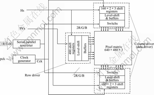
Fig. 1 Block diagram of OLED-on-silicon chip
2.1 Novel pixel circuit
The critical part of the chip design which distinguishes OLEDs from LCD is the pixel or sub-pixel circuit. There are several key points for the pixel design of OLED-on-silicon. Firstly, limited by the production cost, generally, the pixel of the OLED-on-silicon is controlled from 12 μm to 24 μm [7]. So, the pixel circuit must be compact enough to fit the area. Secondly, the operating current of the OLED material is tiny, which brings challenge for the CMOS pixel to display multi-gray scales since generally the current of the CMOS pixel is much greater [4, 8]. Experts of MED Corporation have said that the voltage-programmed pixel is better than the current-programmed pixel in displaying multi-gray scales for OLED-on-silicon in future. Thirdly, the OLED luminance is directly proportional to its current density [9]. With long time operation, the luminance of OLED often decays gradually [10], while ac driving scheme can be used as an electrical compensation to extend the lifetime of OLED [11].
The conventional voltage-programmed two transistors and one capacitor (2T1C) with ac driving scheme seem to be a good choice of OLED-on-silicon [5]. But from the simulating result, we found that there existed switching effect [12] in the pixel circuit during the ac driving, which brings errors to the driving current of OLED and reduces the precision of the display gray scales.
Figure 2(a) shows the conventional 2T1C pixel with the ac driving timing. M1 is the driving transistor that offers current for OLED. M2 is the switch to control the writing of data, which is controlled by the row scan signal Vscan. Cs is the storage capacitor that is used to store the data Vdata. The operation of the pixel is divided into two periods: programming and lighting. During the programming period, M2 turns on and Cs is charged to Vdata. M1 is turned off and OLED is reverse-biased. Then, pixel goes into the lighting period. Now M2 is turned off, the Vdata stored in Cs makes M1 turn on. At this time, OLED is forward biased and lights with the current is offered by M1.
Figure 3 shows the transient simulation result of the 2T1C pixel in Fig. 2(a). The MOSFET SPICE models adopted in the simulation came from the 0.35 μm Dualgate (3.3 V/5 V) CMOS process of CSM. VDD is 5 V, the ratios of M1 and M2 are 0.7 μm/7.5 μm and 2 μm/ 0.5 μm, respectively, and Cs is 0.2 pF. The OLED model is represented by a diode parallel with a capacitor, as the arrow points out in Fig. 2(a). Detailed parameters refer to Ref. [13]. The n is 30, Is is 1×10⁻⁷ A/cm2 for the diode model and the serial resistor R1 is 80 Ω. The capacitance of OLED per unit area is about 25 nF/cm2. One cycle of Vscan is 4 μs. The value of Vdata was set to 0, 1.5, 2.5, 3.5
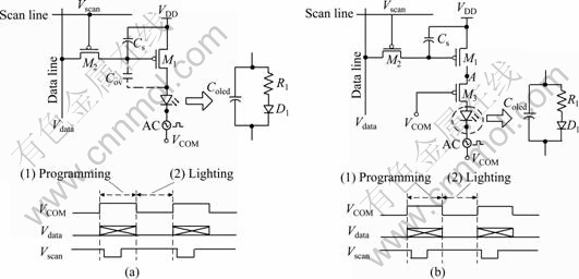
Fig. 2 Conventional 2T1C pixel with ac driving timing (a) and proposed 3T1C pixel for OLED-on-silicon with ac driving timing (b)
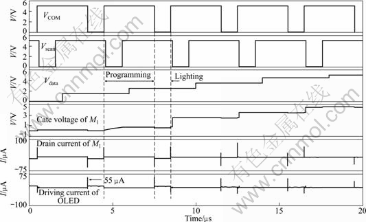
Fig. 3 Transient simulation results of 2T1C pixel with ac driving scheme
and 4.5 V sequentially.
It can be seen from the results above that, the current of OLED during the lighting period varies with the changes of Vdata. The driving current offered by M1 during the lighting period is constant due to the voltage stored on Cs. But, there is a large current glitch of about 55 μA at the moment of co-cathode signal VCOM switching from high to low (i.e. from programming to lighting). The glitch may have no effect on the luminance of OLED when the driving current is high. But, it does affect the luminance of OLED when the driving current is low. The OLED cannot reach the full black state, thus reduce the contrast of display. Additionally, the large glitch would degrade the OLED material [14]. It is analyzed that this glitch is caused by the voltage feedthrough between M1 and Cs at the switch moment of VCOM. When VCOM is switched from high to low, the voltage of M1 drain (connected with OLED) decreases, and at the same time, the decrease is coupled to Cs by the overlap capacitor Cov (the dashed line capacitor in Fig. 2(a)) between the gate and drain of M1. This brings changes to the VGS of M1, which causes the glitch of the driving current.
In order to improve the performance of the 2T1C pixel with ac driving scheme, we propose a voltage- programmed 3T1C pixel, as shown in Fig. 2(b). Compared with 2T1C pixel, the 3T1C pixel only adds a switch M3 between M1 and OLED. The gate of M3 is connected with co-cathode signal VCOM. The operation timing is also shown. Similarly, during the programming period, switch M3 is turned off and the OLED does not work. While in the lighting period, M2 is turned off, M3 turns on, the Vdata stored on Cs makes M1 turn on, and the OLED is forward biased and lights with the driving current are offered by M1. The glitch occurring in 2T1C pixel with ac driving scheme could be reduced effectively with adjusting the ratios of M1 and M3 properly.
The ac simulation result of the proposed 3T1C pixel is shown in Fig. 4. The SPICE models and stimuli used are the same with the simulation of 2T1C pixel in Fig. 3. The ratios of M1, M2 and M3 are 0.7 μm/7.5 μm, 2 μm/0.5 μm and 0.7 μm/9 μm, respectively. Cs is 0.2 pF. As we see from the result, now the current glitch of OLED is effectively reduced to 7.5 μA at the moment of VCOM switching from high to low. The voltage changes of drain of M1 could be shared by the turn on resistance of M3, and the glitch generated by M1 is decreased. Also the overlap capacitor of M3 could absorb current at the moment of M3 turning on, which could furthermore reduce the glitch fed into OLED. In addition, as the voltage swing of gate of M3 (VCOM) is fixed, the current of M3 is stable and would not generate additional glitch.
Figure 5 shows the glitches generated with different ratios of M1 and M3 in 3T1C pixel. Concluded from the simulation results, the glitch can be ideally reduced when the length ratio of M3 to M1, L3/L1 is set between 1 and 1.2, while the widths of M1 and M3 keep the same, i.e. W1=W3. When L3 is small, the equivalent turn on resistance of M3 is low, so that the potential of point A is pulled down immediately at the moment of VCOM switching from high to low. The potential change at point A is coupled to the gate of M1 by its overlap capacitor, which results in the current glitch. As L3 is increased, the turn on resistance of M3 increases also. The speed of potential varied on gate of M1 slows down, which generates smaller glitch. When L3 is increased continually, the charge injected into the channel of M3 generates large current glitch at the moment of VCOM switching from low to high, since the channel charge is proportional to the product of width and length of the MOS transistor [15].
The 3T1C pixel could effectively reduce the current glitch occurring in the 2T1C pixel with ac driving scheme, which could ensure the precision of the driving current and the gray scale of display. The ac driving scheme could offer electrical compensation for the degradation of OLED material. It has simple structure and could easily realize multi-gray scales display with the time ratio grayscale method.
2.2 Row driver, column driver and other functional modules
The OLED-on-silicon chip in this work uses the time ratio grayscale (TRG) method [6] to realize the multi-grayscales display. Each frame of image is divided into n sub-frames, where n is the logarithm to the base 2 of total gray scales. For example, the video data have 6 bit, so one frame is divided into six sub-frames. The lighting time of each sub-frame is set to be 20:21:22:23:24:25. Then, the six sub-frames could totally express 64 gray scales as a whole of one frame period.
As described before, the function of row driver is to generate correct row scan signal to select one of 480 rows of the pixel array. This is mainly implemented with shift registers, as shown in Fig. 6. The output of shift registers is processed by the level shift circuit and driving buffer, then becomes the desired scan signal rscann (subscript n is the number of the selected row), which is connected with the gate of M2 in pixel.
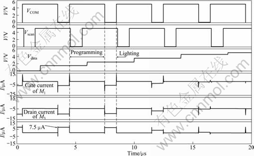
Fig. 4 Simulation result of proposed 3T1C pixel
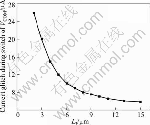
Fig. 5 Glitch of driving current vs varied length of M3 (Width of M1 and M3: 0.7 μm; length of M1: 7.5 μm)
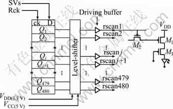
Fig. 6 Block diagram of row driver
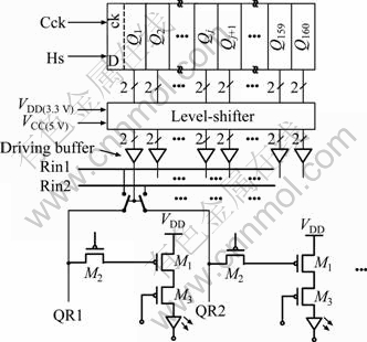
Fig. 7 Block diagram of column driver
Each of the two column drivers generates 160 column scan signals sequentially using shift registers under the control of Hs and Cck, as shown in Fig. 7. Each scan signal controls two groups of data line. That means there are two groups of R/G/B data (such as Rin1/ Gin1/ Bin1, Rin2/Gin2/Bin2) to be written into the adjacent pixels in one cycle of Cck for one column driver. Totally, there are four groups of data to be written. So, the frequency of Cck and the power of the column driver would be effectively reduced. All these are due to the embedded serial-to-parallel conversion module in the OLED-on-silicon chip. The serial-to-parallel conversion module is designed to process the input data into four groups of data so that it could shorten the writing time of pixel data to about one quarter of the situation without it. Another benefit of this module is that it could reduce the numbers of the input pads of the chip, which could reduce the volume and weight of the outer signal lines connected with the chip. This is also favorable for the application of near-to-eye display.
In order to reduce the chip power, both the row and column drivers use clocked circuits and dual power supplies [16]. Two parts with different power supplies are connected with level-shift circuit [17]. For example, the power supply of 480 shift registers in Fig. 6 is 3.3 V, while it is 5 V for the later driving buffers.
3 Tape-out and test
A sample chip with pixel array of 16×3×12 and all the other functional modules extracted from the 640×480 OLED-on-silicon chip design are taped out in MPW (multi-projects wafer) of CSM. The area of the pixel array is 22 μm×22 μm. Figure 8 shows the layout and the taped-out die of the sample chip. Its area is 1 788 μm× 1 988.2 μm and 18 I/O pads are used.
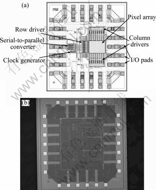
Fig. 8 Sample chip of OLED-on-silicon: (a) Chip layout; (b) Taped-out die
Functional test of the sample chip is done with the testbench shown in Fig. 9. There are mainly three modules in it: video data processing module AD9883, control module based on FPGA and data store module with SRAMs. The datapath of the testbench is as follows. The video data processing module converts the analog video data into digital form. Then, the output will be transformed to the format required by the sub-frames of OLED-on-silicon chip by the control module. Two groups of frame buffers are used as cashes for the data transforming of control module, which operate in ping-ping mode to ensure the continue output of the desired digital video data.
Figure 10 shows the waveforms (snatched by the oscillograph) of several main signals of the chip operating with 8 sub-frames mode. This shows that the chip could work correctly.
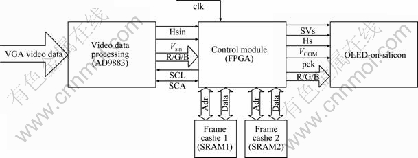
Fig. 9 Testbench of sample chip
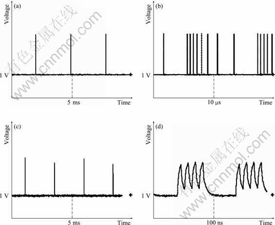
Fig. 10 Functional test of chip: (a) Vs; (b) SVs; (c) Hs; (d) Red video data
4 Conclusions
A low power 640×480 OLED-on-silicon chip design is proposed. Firstly, a novel pixel circuit is proposed. It consists of three transistors and one capacitor (3T1C) that is simple enough for OLED-on-silicon. More importantly, it can effectively reduce the current glitch generated during the ac driving from 55 μA to 7.5 μA, so that it can improve the precision of grayscale of display as well as extend the lifetime of OLED material. Secondly, low power row driver, column driver and other functional modules are also integrated on the chip. Several techniques are adopted to reduce the power consumption and frequency requirement of the chip. Finally, a sample chip with resolution of 16×3×12 is implemented with standard 0.35 μm CMOS process of CSM. The test shows that the chip can operate correctly.
References
[1] LIN Hai-qing, NAVIASKY E, EBNER J, EVANS W, FARRELL P, HUFFORD M, LEVY G, WHEELER D, ALLISON B, PRACHE O. An 852×600 pixel OLED-on-silicon color microdisplay chip using CMOS sub-threshold-voltage-scaling current driver [C]// IEEE, Digest of Technical Papers of ISSCC. USA: IEEE press, 2002, (2): 356-546.
[2] WANG Hong, YU Jun-sheng, LI Lu, TANG Xiao-qing, JIANG Ya-dong. Structure optimization of organic light-emitting devices [J]. Optoelectronics Letters, 2009, 5(2): 0093-0096.
[3] Fan-Chiang K H, YEN Cheng-chi, WU Cheng-hung, CHEN Chien-jung, LIAO Bing-jei, HO Yung-yuan, LIU Chung-yuan, CHEN Yen-chen. LCOS panel using novel color sequential technology [C]// SID Symposium Digest of Technical Papers. USA: SID, 2007, 38(1): 150-153.
[4] HUANG Ran, WANG Xiao-hui, WANG Wen-bo, DU Huan, HAN Zheng-sheng. Design of a 16 gray scales 320×240 pixels OLED-on-silicon driving circuit [J]. Journal of Semiconductors, 2009, 30(1): 015010-1-4.
[5] SI Yu-juan, ZHAO Yi, CHEN Xin-fa, LIU Shi-yong. A simple and effective ac pixel driving circuit for active matrix OLED [J]. IEEE Transactions on Electron Devices, 2003, 50(4): 1137-1140.
[6] SHIN D Y, WOO J K, HONG Y, KIM K N, KIM D I, YOO M H, KIM H D, KIM S. Reducing image sticking in AMOLED displays with time-ratio gray scale by analog calibration [J]. Journal of the Society for Information Display, 2009, 17(9): 705-713.
[7] LIU Yan-yan, GENG Wei-dong, DAI Yong-ping. The restraining of switch effects in AC driving pixel circuit of OLED-on-silicon [J]. Optoelectronics Letters, 2010, 6(2): 0112-0115.
[8] PARK C Y, LEE S H, HYUN C H, KANG S K, KWAK B C, LIM H S, KWON O K, CHUNG H K. High efficient top emitting OLED micro display for personal display application [C]// Proceeding of the 17th International Display Workshops. Japan: ITE and SID, 2010: 327-330.
[9] ASHTIANI S J, NATHAN A. A driving scheme for active-matrix organic light-emitting diode displays based on current feedback [J]. Journal of Display Technology, 2009, 5(7): 257-264.
[10] ZARDAREH S Z, BOROUMAND F A. Degradation in organic light emitting diodes [J]. Journal of World Academy of Science, Engineering and Technology, 2009, 50: 274-277.
[11] SHEN J, WANG D, LANGLOIS E, BARROW W A, GREEN P J, TANG C W, SHI J. Degradation mechanisms in organic light emitting diodes [J]. Synthetic Metals, 2000, 111/112: 233-236.
[12] WEGMANN G, VITTOZ E A, FOUAD R. Charge injection in analog MOS switches [J]. Journal of Solid-state Circuits, 1987, SC-22(6): 1091-1097.
[13] DAWSON R M A, SHEN Z, FURST D A, CONNOR S, HSU J, KANE M G, STEWART R G, IPRI A, KING C N, GREEN P J, FLEGAL R T, PEARSON S, BARROW W A, DICKEY E, PING K, ROBINSON S, TANG C W, van SLYKE S, CHEN F, SHI J, LU M H, STURM J C. The impact of the transient response of 0rganic light emitting diodes on the design of active matrix OLED displays [C]// IEDM’98 Technical digest, International. USA: IEEE Press, 1998: 875-878.
[14] SOH K M, KLEIN S, HITZELBERGER C, XU Chi-hao. Electrical and optical characterization of PM OLED displays [C]// Proceeding of the Twenty-Fifth International Display Research Conference, EuroDisplay 2005. USA: SID, 2005: 393-396.
[15] BAKER R J. CMOS Circuit Design, Layout, and Simulation [M]. Third Edition. USA: Wiley-IEEE Press. 2011: 339-340.
[16] JIN Li-yan, LEE J H, HA P B, KIM Y H. Design of logic process based low-power 512-bit EEPROM for UHF RFID tag chip [J]. Journal of Central South University of Technology, 2010, 17(5): 1011-1020.
[17] PAN Xue-wen, ZHOU Ji-cheng, ZHENG Xu-qiang. A level-shifting circuit based on low-voltage rail-to-rail CMOS op-amp [J]. Journal of Central South University of Technology: Science and technology, 2010, 41(4): 1473-1478. (in Chinese)
(Edited by YANG Bing)
Foundation item: Project(10ZCKFGX00200) supported by the Tianjin Science and Technology Supporting Plan, China; Project supported by the Fundamental Research Funds for the Central Universities of China
Received date: 2011-02-15; Accepted date: 2011-05-27
Corresponding author: LIU Yan-yan, PhD; Tel: +86-22-23498590; E-mail: lyytianjin@nankai.edu.cn

