Trans. Nonferrous Met. Soc. China 22(2012) s781-s786
Material properties and machining performance of hybrid Ti2AlN bulk material for micro electrical discharge machining
Eui-Seong CHOI 1, Jinwoo SUNG1, Qi-min WANG2, Kwang-Ho KIM 1, Ahmed BUSNAINA3, Myung Chang KANG 1
1. National Core Research Center for Hybrid Materials Solution, Pusan National University, Busan 609-735, Korea;
2. School of Mechanical and Electronic Engineering, Guangdong University of Technology, Guangzhou 510006, China;
3. Department of Mechanical and Industrial Engineering, College of Engineering, Northeastern University, Boston MA 02115, USA
Received 21 May 2012; accepted 20 November 2012
Abstract: Mn+1AXn (MAX) phases are a family of nanolaminated compounds that possess unique combination of typical ceramic properties and typical metallic properties. As a member of MAX phase, Ti2AlN bulk materials are attractive for some high- temperature applications. The synthesis, characteristics and machining performance of hybrid Ti2AlN bulk materials were focused on in this work. The bulk samples mainly consisting of Ti2AlN MAX phase with density close to theoretic one were synthesized by a spark plasma sintering method. Scanning electron microscopy results indicate homogenous distribution of Ti2AlN grains in the samples. Micro-hardness values are almost constant under different loads (6-6.5 GPa). A machining test was carried out to compare the effect of material properties on micro-electrical discharge machining (micro-EDM) performance for Ti2AlN bulk samples and Ti6242 alloy. The machining performance of the Ti2AlN sample is better than that of the Ti6242 alloy. The inherent mechanism was discussed by considering their electrical and thermal conductivity.
Key words: hybrid Ti2AlN bulk; micro-electrical discharge machining; electrical conductivity; micro-hole shape
1 Introduction
Advanced bulk materials with unique metallurgical properties, such as titanium alloys, ceramics, stainless steels, and other superalloys, were developed to meet the demands of extreme applications. Along with making these materials harder, tougher, less heat sensitive and/or more resistant to corrosion and fatigue, they also became more difficult to be machined [1,2]. Non-traditional machining methods, such as electrical discharge machining (EDM), were employed to machine difficult-to-cut materials [3]. As well known, the workpiece material is removed by thermal melting and vaporization during the EDM process.
Mn+1AXn (abbreviated as MAX, where M is an early transition metal, A is an IIIA- or IVA- group element, X is C or N, and n=1, 2, or 3) phases are a family of nanolaminated compounds with Mn+1Xn layers being mixed metallic-covalent nature of the strong M-X bonds and weaker M-A bonds, and the MAX phases possess unique combination of typical ceramic properties (e.g., high melting point, and good corrosion resistance) and typical metallic properties (e.g., good thermal and electrical conductivity). This unique combination of properties makes MAX phases fascinate for potential application to high temperature components and electrical contacts, etc [1,3].
As one member of nanolaminated MAX phases, hybrid Ti2AlN bulk material was paid great attention in recent years. WANG and ZHOU [4] and BARSOUM et al [5] fabricated bulk Ti2AlN by hot isostatic pressing (HIP) or spark plasma sintering (SPS) of mixing elemental or binary powders at high temperatures (1200-1600 °C). In the last ten years, not only the electronic [6,7] and crystalline structures of Ti2AlN compound [8], but also the mechanical [4,9], electronic [10], thermal [11], tribological [12], and corrosive properties [13] of the bulk, no actual test was found in the micro-EDM applications on the hybrid Ti2AlN bulk sample up to the present.
In this work, hybrid Ti2AlN bulk samples were fabricated using a spark plasma sintering method from mixture of Ti, Al, and TiN powders. The material properties and machining performance were investigated for Ti2AlN bulk samples and Ti6242 alloy. And, micro-EDM based on the resistance capacitance (RC) discharged circuit was conducted to investigate the machining performances of Ti2AlN bulk samples by varying the discharge voltages. The optical characterization of machined micro-holes was verified by field emission scanning electron microscope (FE-SEM).
2 Experimental
2.1 Preparation and characterization of Ti2AlN material
The powders of Ti (99.5% purity, 10 μm), Al (99.8% purity, 3 μm), and TiN (99.5% purity, 3 μm) were used as starting materials for sintering the Ti2AlN bulk specimens. The powders with a designed compositions of n(Ti):n(Al):n(TiN)=1:1:1 were firstly mixed in an attrition milling machine (KMDC-1BV) at a rotating speed of 200 r/min for 1.5 h. During mixing, the mixing chamber was vacuumed and filled with Ar gas to protect the powders from oxidation, and stainless steel balls with the diameter of 5 mm were filled into the chamber to increase the mixing efficiency. The mixed powders were pre-pressed into graphite dies with the diameter of 30 mm and put into the spark plasma sintering machine (Dr. Sinter, SPS SYNTEX INC). The samples were heated to 1250 °C in less than 20 min by controlling the applying voltage at a vacuum of 0.3 Pa. The soaking time was 10 min with an applied pressure of 30 MPa.
The sintered products were sliced into coupons with a thickness of 1.5 mm and then ground to 2500 grit, polished and cleaned. The density of the bulk sample was obtained by an Archimedes method. The microhardness was measured using a Vickers indenter. The morphology and phase structure of the powders and the samples were investigated by a scanning electron microscope (SEM, S-4800N, Hitachi, Japan) and an X-ray diffractometer (D8 Advance, Bruker) with monochromatic Cu Kα radiation operated at 40 kV. The thermal conductivity was not measured by the laser flash method and electrical resistivity was not measured by the four-point probe method. The data were from previous works [14,15].
2.2 EDM tests of Ti2AlN material
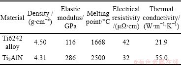
The EDM tests of the specimens were performed on a die-sinking EDM machine model type Hyper-15, made by Hybrid Precision Co., in Korea. The maximum travel range of the machine was 260 mm (X) × 10 mm (Y) × 100 mm (Z) with the resolution of 0.1 μm in X, Y and Z directions. The electrode was tungsten (W) rod with a diameter of 300 μm. The dielectric fluid (Oelheld, IME-MH) having relatively high flash point, high auto-ignition temperature and high dielectric strength was cycled by a pump and stirred by an agitator to ensure that the particles were suspended uniformly within the dielectric fluid. A series of experiments were carried out using a RC-circuit to evaluate the characteristics of the machined holes. The resistance was set at 1 kΩ, and the voltage and condenser were varied. The voltages of 150, 200 and 250 V and capacitor of 10000 pF were chosen, respectively. For the electrode, the feed rate was 10 m/s and the spindle speed was 1000 r/min. By directly comparing the material properties on micro-EDM, the workpiece used in each test was the Ti6242 alloy and Ti2AlN sample with a thickness of 1400 μm. Ti alloy can be classified as a difficult-to-cut material, not suitable for traditional machining [1]. The difference between their melting points, electrical resistivity and thermal conductivity are presented in Table 1 [14,15].
As shown in Table 1, the elastic modulus, melting point of Ti2AlN is much higher than that of the Ti6242 alloy. Therefore, Ti2AlN material is more promising for application as structural materials at high-temperatures than Ti alloys. At the same time, the electrical and thermal conductivity of Ti2AlN is close, even a bit higher than that of Ti6242 alloy.
Table 1 Material properties comparison between Ti6242 alloy and Ti2AlN bulk material
3 Results and discussion
3.1 Material properties of Ti2AlN samples
Figure 1 shows the second electron SEM images of the Al, Ti and TiN powders for sintering Ti2AlN materials. It can be seen from Fig. 1 that the Al powers exhibit spherical morphologies, with particle size in the range of 2-5 μm. Ti powers exhibit angular morphologies, with particle size in the range of 5-20 μm.
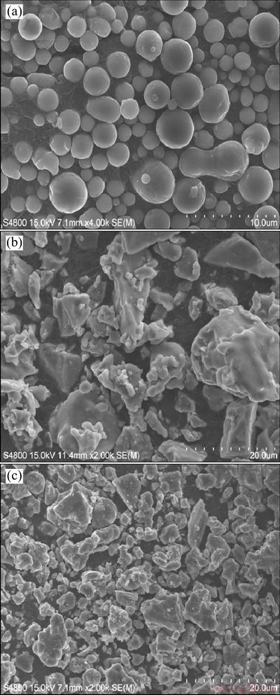
Fig. 1 Second electron SEM images of Al (a), Ti (b) and TiN (c) powders for sintering Ti2AlN samples
TiN powders also have angular shape, but with particle sizes ranging from 2-10 μm.
The XRD patterns in Fig. 2(a) reveal that the mixed powders are fully composed of Al, Ti and TiN phases, which exhibit the same XRD peaks from original Al, Ti and TiN powders. No other phase forms during mixing in the attrition milling machine. Figure 2(b) shows the XRD pattern of the mixture of raw powders of Ti+Al+TiN at about 1250 °C for 10 min. It can be seen that pure Ti2AlN phase appears in the sintered specimen. Random orientation characteristics and good crystallization of the Ti2AlN phase are observed in Fig. 2(b). Obviously, the reaction of Ti+Al+TiN→Ti2AlN occurs during spark plasma sintering, which results in the formation of polycrystalline Ti2AlN materials.
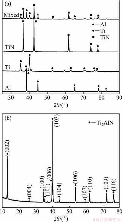
Fig. 2 XRD patterns of original and mixed powders (a) and XRD pattern of original powders and sintered Ti2AlN samples (b)
Figures 3(a) and (b) show the SEM images of the fractured (secondary electron image) and polished (backscattered electron image) cross-sections of the Ti2AlN specimens sintered by the SPS technique. In Fig. 3(a), it can be seen that the crystals with a dense and lamellate structure are well developed. Plate-like grains with the width of 2-4 μm and the length of 5-10 μm are observed. In Fig. 3(b), the polished image of the cross-section indicates that the sintered Ti2AlN specimen is dense, with only a few pores and oxide inclusions being observed. The density of the sintered Ti2AlN material is measured to be 4.25-4.34 g/cm3 by Archimedes method, close to the theoretical density of the Ti2AlN material (4.31 g/cm3).
Figure 4 shows the Vickers hardness of the sintered Ti2AlN samples. It can be seen that the hardness value (6-6.5 GPa) is almost constant under different loads, which is larger than that of the Ti alloys (3-4 GPa), and far less than that of TiN ceramics (18-21 GPa). This value is a bit higher than that in Ref. [16]. The reason may lie in the oxidation inclusions (Fig. 3(b)).
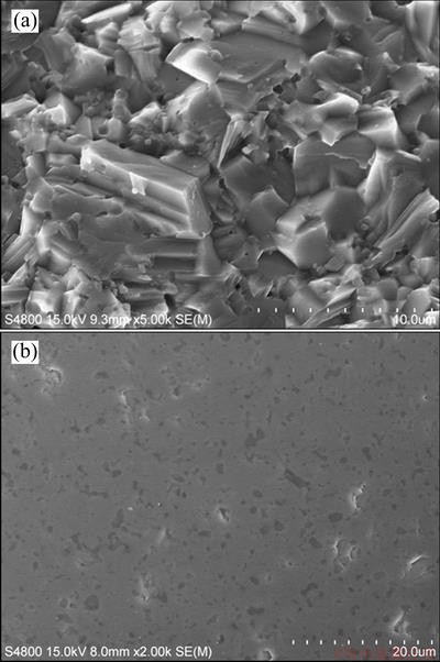
Fig. 3 SEM images fractured cross-section (a) and polished cross-section (b)
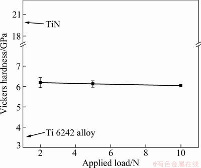
Fig. 4 Vickers hardness of sintered Ti2AlN samples
3.2 Micro-EDMed performance of Ti2AlN workpiece
The electrical discharge machining is removed by the thermal melting and vaporization during machining of conductive materials. The surface integrity is mainly decided by eroded craters that are proportional to the single discharge energy [2]. For a resistance capacitance circuit, energy is a function of capacitance and voltage. The higher the energy is, the larger the crater size is and hence the greater the material remove rate is [1,2].
Figure 5 shows the FE-SEM images on the surface shape of micro-holes for Ti6242 alloy and Ti2AlN workpiece discharge voltages of 150, 200 and 250 V when a capacitance is 10000 pF. As expected, with the increase of voltage, the dimensional accuracy and roundness error of the micro-holes become worse for both materials. This is why the discharges strike the surface of the workpiece more intensely with increase of discharge voltage, and the resulting worsened erosion effect leads to a deterioration of the surface shapes [1-3].
Furthermore, an extended discharge voltage allows greater discharge energy to melt and penetrate deeper into the material, which produces deeper and larger craters, causing an increase of the surface integrity on the workpiece. For comparison of both material properties, it can be seen that Ti2AlN workpiece consistently results in good dimensional accuracy and roundness error. This trend seems to be material properties that result from good thermal and electrical conductivity. Also, good machinability results from the formation of polycrystalline Ti2AlN materials as shown in Figs. 2 and 3. Conversely, the Ti alloy results in the poor performance of EDM process. Consequently, the workpiece material is removed by thermal melting and vaporization during the EDM process, and the EDM characteristics of the workpiece depend on its thermal properties and electrical properties. Also, the machining performance of EDMed workpiece is not largely influenced by the magnitude of micro-hardness and melting point in this experiment. These results are consistent with the characteristics reported in Refs. [17,18].
Figure 6 shows the comparison of machining time and electrode wear for Ti6242 alloy and Ti2AlN workpiece at three discharge voltages (150, 200 and 250 V). According to Fig. 6, machining time decreases and electrode wear increases with the increase of discharge voltage for both specimens because discharge energy increases with the increase of voltages, generating a very high temperature within the plasma channel. This high temperature causes a large impulse force to repel debris from the crater in the dielectric fluid. The gap distance also increases with increasing discharge voltage, and smoothly repelling melt material from the crater in the dielectric fluid [2,17]. Moreover, Ti2AlN workpiece shows superior machining time and electrode wear that is led by its homogenous distribution crystallization and higher electrical and thermal conductivity compared with conventional Ti6242 alloy. Consequently, the applicability in the micro-EDM of hybrid Ti2AlN material is proved.
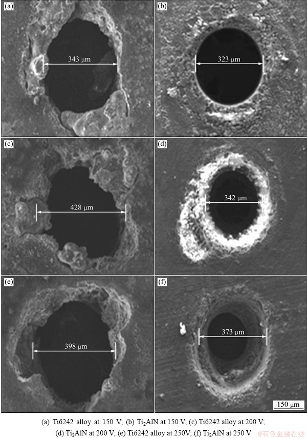
Fig. 5 FE-SEM image of Ti6242 alloy and Ti2AlN materials according to μ-EDM voltage value
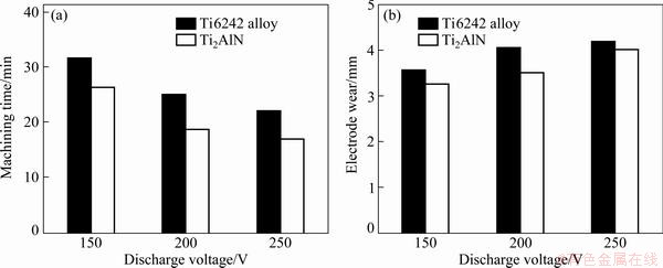
Fig. 6 Machining characteristics of machining time (a) and electrode wear (b) according to discharge value for Ti6242 alloy and Ti2AlN samples
4 Conclusions
The hybrid Ti2AlN bulk was synthesized utilizing a spark plasma sintering method. The synthesized Ti2AlN bulk shows crystallite structure and MAX phase. Scanning electron microscopy results indicate the homogenous distribution of Ti2AlN grains in the samples. The micro-hardness (6-6.5 GPa) is almost constant under different loads. The machining performance of the EDMed micro-hole of Ti2AlN sample is significantly superior to that of Ti6242 alloy due to its homogenous distribution crystallization and higher electrical and thermal conductivity in point of dimensional accuracy and roundness error of workpiece and machining time and electrode wear.
References
[1] LI Mao-sheng, CHI Guan-xin, WANG Zhen-long, WANG Yu-kui, DAI Li. Micro electrical discharge machining of small hole in TC4 alloy [J]. Transactions of Nonferrous Metals Society of China, 2009, 19: 434-439.
[2] TAK H S, HA C S, LEE H J, LEE H W, JEONG Y K, KANG M C. Characteristic evaluation of Al2O3/CNTs hybrid materials for micro-electrical discharge machining [J]. Transactions of Nonferrous Metals Society of China, 2011, 21: 28-32.
[3] LIU C C. Microstructure and tool electrode erosion in EDMed of TiN/Si3N4 composites [J]. Mater Sci Eng A, 2003, 363: 221-227.
[4] WANG J Y, ZHOU Y C. Recent progress in theoretical prediction, preparation, and characterization of layered ternary transition-metal carbides [J]. Ann Rev Mater Res, 2009, 39: 415-443.
[5] BARSOUM M W, EI-RAGHY T, ALI M. Processing and characterization of Ti2AlC, Ti2AlN, and Ti2AlC0.5N0.5 [J]. Metall Mater Trans A, 2000, 31: 1857-1865.
[6] YAN M, MEI B C, ZHU J Q, TIAN C G, WANG P. Synthesis of high-purity bulk Ti2AlN by spark plasma sintering (SPS) [J]. Ceram Int, 2008, 34: 1439-1442.
[7] HUG G, JAOUEN M, BARSOUM M W. X-ray absorption spectroscopy, EELS, and full-potential augmented plane wave study of the electronic structure of Ti2AlC, Ti2AlN, Nb2AlC, and (Ti0.5Nb0.5)2AlC [J]. Phys Rev B, 2005, 71: 024105.
[8] DJEDID A,  A, ABBES O, ABBAR B. Theoretical investigations of structural, electronic and thermal properties of Ti2AlX(X=C,N) [J]. Physical B, 2009, 404: 3475-3482.
[9] FARBER L, LEVIN I, BARSOUM M W, EL-RAGHY T, TZENOV T. High-resolution transmission electron microscopy of some Tin+1AXn compounds (n=1, 2; A=Al or Si; X=C or N) [J]. J Appl Phys, 1999, 86: 2540.
[10] MANOUN B, ZHANG F X, SAXENA S K, EI-RAGHY T, BARSOUM M W. X-ray high-pressure study of Ti2AlN and Ti2AlC [J]. J Phys Chem Solids, 2006, 67: 2091-2094.
[11] SALAMA I, EI-RAGHY T, BARSOUM M W. Synthesis and mechanical properties of Nb2AlC and (Ti,Nb)2AlC [J]. J Alloy Compd, 2002, 347: 271-278.
[12] LIAO T, WANG J Y, ZHOU Y C. Basal-plane slip systems and polymorphic phase transformation in Ti2AlC and Ti2AlN: A first-principles study [J]. J Phys Condes Matter, 2006, 18: 6183-6192.
[13] LIAO T, WANG J Y, ZHOU Y C. Deformation modes and ideal strengths of ternary layered Ti2AlC and Ti2AlN from first-principles calculations [J]. Phys Rev B, 2006, 73: 214109-1-7.
[14] SCABAROZI T, GANGULY A, HETTINGER J D, LOFLAND S E, AMINI S, FINKEL P, EL-RAGHY T, BARSOUM M W. Electronic and thermal properties of Ti3Al(C0.5N0.5), Ti2Al(C0.5N0.5) and Ti2AlN [J]. J Appl Phys, 2008, 104: 073713-1-6.
[15] BARSOUM M W, ALI M, EL-RAGHY T. Processing and characterization of Ti2AlC, Ti2AlN and Ti2AlC0.5N0.5 [J]. Metall Mater Trans A, 2000, 31: 1857-1865.
[16] LIN Z J, ZHUO M J, LI M S, WANG J Y, ZHOU Y C. Synthesis and microstructure of layered-ternary Ti2AlN ceramic [J]. Scr Mater, 2007, 56: 1115-1118.
[17] XIE Bao-cheng, WANG Yu-kui, WANG Zhen-long, ZHAO Wang-sheng. Numerical simulation of titanium alloy machining in electric discharge machining process [J]. Transactions of Nonferrous Metals Society of China, 2011, 21: 434-439.
[18] FONDA P, WANG Zhi-gang, YAMAZAKI K, AKUTSU Y. Fundamental study on Ti-6Al-4V’s thermal and electrical properties and their relation to EDM productivity [J]. J Mater Process Technol, 2008, 202: 583-589.
(Edited by CHEN Wei-ping)
Foundation item: Project supported by a 2-Year Research Grant of Pusan National University, Korea; Project (2010-0008-277) partly supported by NCRC Program funded by the Ministry of Education, Science and Technology
Corresponding author: Myung Chang KANG; Tel: +82-51-510-2361; E-mail: kangmc@pusan.ac.kr
DOI: 10.1016/S1003-6326(12)61804-4