Influence of sputtering parameters on microstructure and mechanical properties of GeSbTe films
FU Yong-zhong(付永忠)
Micro/Nano Science and Technology Center, Jiangsu University, Zhenjiang 212013, China
Received 8 March 2007; accepted 2 July 2007
Abstract: GeSb2Te4 films were deposited on Si substrates by RF magnetron sputtering, and the effects of sputtering power on the surface topography and anti-compression properties were studied with atomic force microscope(AFM) and nanoindenter. Meanwhile, the mechanical properties of GeSb2Te4 films with oxygen impurity were also investigated. The results indicate that proper sputtering power is important for obtaining GeSb2Te4 films with high compact structure and low surface roughness, which present good load-support capacity. Although the effect of oxygen impurity on the anti-compression properties of GeSb2Te4 films is not very significant as a whole, certain oxygen dosage can relax the internal stress, thereby the hardness of the films drops slightly.
Key words: GeSbTe films; sputtering parameters; microstructure; mechanical properties
1 Introduction
Nanometer and atomic scale surface modification on phase-change films using scanning probe microscope(SPM) is a new and promising method to store data with ultra-high density[1-2]. Although the optical and electrical properties of chalcogenide semiconductor have been addressed by many literatures[3-5], its mechanical properties have been rarely reported, especially, the effects of sputtering technical parameters on them have not been addressed so far. Noting that using tip-inducing phase change storage is a contact storage method, it is necessary to investigate the mechanical properties such as anti-compression while studying electric-inducing phase change on the material. Herein, atomic force microscope(AFM) and nanoindenter were employed to characterize surface topography and their mechanical properties of GeSb2Te4 films deposited with different sputtering powers and oxygen impurity. Thereby, a base is laid to study the phase change storage mechanism of GeSb2Te4 films and their disc production.
2 Experimental
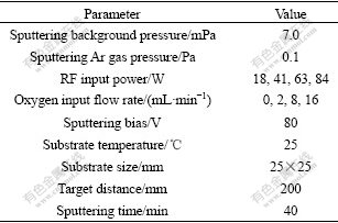
The GeSb2Te4 films were deposited on Si(111) substrates by RF magnetron sputtering equipment, and the compound target with 60 mm in diameter was provided by Mitsubishi Corporation. Two groups of samples were prepared in the experiment. One group alters the sputtering power with other parameters unchanged, and the detailed sputtering parameters are listed in Table 1. The other mainly makes the oxygen input flow vary at the sputtering power of 41 W.
Table 1 Sputtering parameters of GeSb2Te4 films

DI Nanoscope Ⅲ SPM was employed to analyze the surface topography of prepared GeSb2Te4 films. Nanoindention was conducted with a TriboIndenter system provided by Hysitron Company. The indent tip employed was diamond Cono-Spherical tip, the apex radius of which is about 2 μm. Nanoindention test result was the average value obtained from four individual tests in different parts of the sample to ensure the reliability. All the tests were conducted on ambient condition.
3 Results and discussion
3.1 Effect of sputtering power
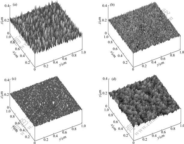
When the sputtering power is not very high, the incident kinetic energy of atoms sputtered onto the substrate is comparatively small due to its own low energy, which leads to low surface transfer rate. Thus the film can easily present three-dimension growth mode, resulting in relatively high surface roughness, as shown in Fig.1(a). With the increment of the power, the roughness deceases, and the amount of island grains increases significantly with the drop of its roughness. In other words, the microstructure of GeSb2Te4 films becomes stable gradually. It can be seen from Fig.1(c) that at sputtering power of 63 W, the film surface has been quite smooth and compact, and the grains go much smaller. This should be ascribed to the growth transformation from three-dimension mode to two- dimension one, which makes for the optimization of the structure of the film[6]. Too high power will reduce the surface quality of GeSb2Te4 films owing to the fact that part of the high energy sputtering particles caused by higher sputtering power collide intensively with the deposited film on the substrate, and the high energy particles play the role of etching the film in some degree accordingly[7-8]. Consequently, this will block the two- dimension growth of GeSb2Te4 film, and the surface quality of films is much affected, as shown in Fig.1(d).

Fig.1 AFM images of GeSb2Te4 film deposited with different sputtering powers: (a) 18 W; (b) 41W; (c) 63 W; (d) 84 W
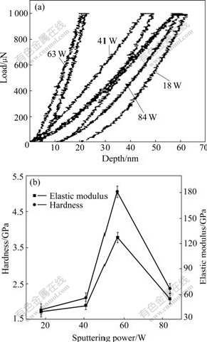
The hardness and elastic modulus values of the film are mainly obtained by analyzing the load― displacement curves of the loading and unloading process with the nanoindenter[9], thereby the load supporting capacity of tested film can be reflected. Fig.2(a) shows the load―displacement curves of GeSb2Te4 film deposited by different sputtering powers. Fig.2(b) indicates that the hardness and elastic modulus of GeSb2Te4 films increase with the increment of sputtering power when other parameters are unchanged. At the same time, considering that the two measured values drop obviously at the power of 84 W, it is believed that there must be an optimum power for the mechanical properties of GeSb2Te4 film.

Fig.2 Effect of sputtering power on hardness and elastic modulus of GeSb2Te4 film: (a) Load―depth curves; (b) Varia- tion curves of hardness and elastic modulus with sputtering power
Generally speaking, the internal dislocation density or the structural compaction of the film may be taken into account to analyze the hardness and elastic modulus measured with nanoindenter[10-11]. However, the deposited GeSb2Te4 film by RF magnetron sputtering possesses the amorphous structure. In this case, The mechanical properties of the film should be emphasized particularly on the deformation mechanism of the material under the indenter[12].
Supposing that Re, Rs and Rd are resistances to compression, shear and compaction or densification for the GeSb2Te4 film underloading of indenter, respectively. The resistance for the deformation, R, would be overlapping of these resistances. Thus their relationship can be written as
R∝(ReRsRd) (1)
On this basis, MAKISHIMA and MACKENZIE[13] gave the simplified formulae to calculate the hardness H and elastic modulus E of amorphous glassy material:
 (2)
(2)
 (3)
(3)
where ρp and G are the packing density of atoms and bonding energy per unit volume, respectively; β is a coefficient directly related to bond strength, and C is a constant.
The above equations mean that the anti- compression properties of the amorphous GeSb2Te4 film greatly depend on the density of its internal packing atoms or the bond strength; in other words, the bigger the packing density or the bonding energy per unit volume of the film, the higher the values of hardness and elastic modulus of the material. So the previous experiment results, combined with the microstructure discussed before, can be considered with the increment of the compaction of the film accordingly. The density of the atoms and the bonding energy increase, so the film has high internal energy density. It is also well accepted that the indent tip must separate the bond between atoms in order to penetrate the material during nanoindention. Thus, the film with higher internal energy density will present certain anti-compression capacity.
YEN[14] also discovered several solid materials whose hardness has a close relation with the density of the atoms and the bond energy. According to the energy density theory, they deemed that classical hardness should be related to the bond density. As to the drop of the hardness and elastic modulus values at the power of 84 W, it may be due to the loose structure caused by too much high energy sputtering particles or oxidation.
3.2 Effect of oxygen impurity
The surface compositions of GeSb2Te4 films deposited with different oxygen flow rates were analyzed by EDX. Evidently, the oxygen content increases in different degree with the increment of the oxygen input flow rate, especially, the content is more distinct at 16 mL/min. Besides, even there is no oxygen input during the process of sputtering, the composition of GeSb2Te4 film, sometimes, still has certain oxygen, due to the degasification of the target clamp caused by the large quantity of heat, which arises from the target and its clamp when the power is comparatively high[15].
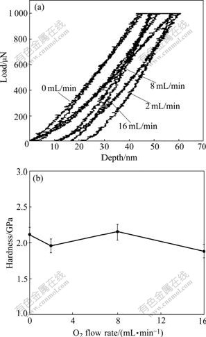
Nanoindention results indicate that the effect of oxygen impurity content on the hardness values of GeSb2Te4 films is not as marked as that of the power. The hardness, as a whole, varies between 1.8 and 2.2 GPa, and there is no obvious variation trend (Fig.3). However, the hardness value at certain oxygen content is under the average one. For example, the hardness values at oxygen input flow rate of 2 mL/min and 16 mL/min are lower than that with no oxygen input, about 0.15 GPa and 0.23 GPa, respectively.

Fig.3 Effect of oxygen amount on hardness of GeSb2Te4 films:(a) Load―depth curves; (b) Variation curves of hardness with O2 flow rate
On one hand, as addressed in Ref.[16], most of the deposited GeSbTe films are in the residual stress state, so part of the oxygen atoms relax the internal stress between Ge-Te, Ge-Sb and Sb-Te structures, thereby the anti-compression capability will decrease to some extent; On the other hand, the oxidation becomes more severe when the extra oxygen is input leading to the looser film structure[17]. In addition, it should be pointed out that the sputtering process is quite unstable when the oxygen is imported into the chamber. Moreover, whether the unstable factor influences the result is still unclear at present, and further research work is under way.
4 Conclusions
1) The compaction of the film goes higher increasingly with the increment of the sputtering power, and the surface roughness becomes smaller due to two- dimension growth mode of the film. Moreover, the anti-compression capacity increases markedly.
2) Too high power is liable to the decrease of the densification of the film, the surface quality and the mechanical properties of the film as well. The energy density theory is adopted to explain the mechanism.
3) The effect of oxygen content on the hardness of GeSb2Te4 films is not as significant as that of sputtering power. However, the hardness of the GeSb2Te4 films with certain oxygen content drops slightly due to the relaxation of its internal stress.
References
[1] WRIGHT C D, ARMAND M, AZIZ M M. Terabit-per-square-inch data storage using phase-change media and scanning electrical nanoprobes [J]. IEEE Transactions on Nanotechnology, 2006, 5(1): 50-61.
[2] SUGAWARA K, TANAKA K, GOTOH T. Scanning tunneling microscope modifications of amorphous Ge-Sb-Te films[J]. J Non-Cryst Solids, 2003, 326: 37-41.
[3] ZHANG Guang-jun, GU Dong-hong, GAN Fu-xi. Study on the optical properties and erasing performance of Ge2Sb2Te5 phase change thin films [J]. Acta Photonica Sinica, 2005, 34(4): 576-581.
[4] HENDRIK F H, MARIN O B, YVES C M, MICHAEL B, KUMAR H W. Ultra-high-density phase-change storage and memory [J]. Nature Materials, 2006, 5(5): 383-387.
[5] GOTOH T, SUGAWARA K, TANAKA K. Nanoscale electrical phase-change in GeSb2Te4 films with scanning probe microscope [J]. J Non-Cryst Solids, 2002, 29B: 968-972.
[6] YANG Lie-yu, GUAN Wen-duo, GU Zhuo-ming. The film technique of material surfaces [M]. Beijing: Renmin Jiaotong Press, 1991. (in Chinese)
[7] XU Xiao-hong, WU Hai-shun, ZHANG Fu-qiang, ZHANG Cong-jie, LI Zuo-yi. Study on deposition rate of AlN thin films using reactive magnetron sputtering [J]. Rare Metal Materials and Engineering, 2002, 31(3): 209-212. (in Chinese)
[8] FU Yong-zhong, DING Jian-ning, YANG Ji-chang, XIE Guo-xin. GeSb2Te4 film surface and mechanical property characterized by fractal [J]. Journal of Vacuum Science and Technology, 2006, 26(4): 282-285. (in Chinese)
[9] ZHANG Tai-hua. The testing technology and application on micro/nano meter mechanical properties [M]. Beijing: China Machine Press, 2005. (in Chinese)
[10] OLIVER W C, PHARR G M. Measurement of hardness and elastic modulus by instrumented indentation: Advances in understanding and refinements to methodology [J]. J Mater Res, 2004, 19(1): 3-20.
[11] CHENG Yun-jun, LI Shi-qiong, LIANG Xiao-bo, ZHANG Jian-wei. Effect of deformed microstructure on mechanical properties of Ti-22Al-25Nb alloy [J]. Trans Nonferrous Met Soc China, 2006, 16(3): 2058-2069.
[12] CHRISTOVA K, MANOV A, PAMUKCHIEVA V. Mechanical stress studies of amorphous GexSb40-xS60 film [J]. J Non-Cryst Solids, 2003, 325: 142-149.
[13] MAKISHIMA A, MACKENZIE J D. Hardness equation for ormosils [J]. Journal of Sol-gel Science and Technology, 2000, 19(3): 627-630.
[14] YEN C H. Correlation of hardness with atomic number density and bond energy density [D]. Cleveland, OH: Case Western Reserve University, 1985.
[15] DIMITROV D, SHIEH H. The influence of oxygen and nitrogen doping on GeSbTe phase-change optical recording media properties [J]. Materials Science and Engineering, 2004, 107B: 107-112.
[16] JONG C A, FANG W L, LEE C M. Mechanical properties of phase change recording media: GeSbTe films [J]. Jpn J Appl Phys, 2001, 40: 3320-3325.
[17] GU Si-peng, HOU Li-song LIU Bo, CHEN Jing. Optical and structural properties of oxygen-doped and annealed Ge-Sb-Te thin films [J]. Chinese Journal of Laser, 2004, 30(12): 1111-1114. (in Chinese)
Foundation item: Project(50475124) supported by the National Natural Science Foundation of China; Project(200330) supported by the Foundation for the National Excellent Doctoral Dissertation of China; Project(NCET-04-0515) supported by the New Century Excellent Talents in University, China
Corresponding author: FU Yong-zhong; Tel:+86-511-88780244; E-mail: yzfu@ujs.edu.cn
(Edited by YANG Bing)