Trans. Nonferrous Met. Soc. China 22(2012) s89-s94
Synthesis of hierarchical hollow spherical CdS nanostructures by microwave hydrothermal process
HU Bao-yun1, JING Zhen-zi1, HUANG Jian-feng2, YUN Jun3
1. School of Materials Science and Engineering, Tongji University, Shanghai 201804, China;
2. Key Laboratory of Auxiliary Chemistry and Technology for Chemical Industry, Ministry of Education, Shaanxi University of Science and Technology, Xi’an 710021, China;
3. School of Environmental Science and Engineering, Shanghai Jiao Tong University, Shanghai 200240, China
Received 9 July 2012; accepted 16 August 2012
Abstract: Hierarchical hollow spherical CdS nanostructures were synthesized via a simple microwave hydrothermal(M-H) process using CdCl2・H2O and Na2S2O3・5H2O as raw materials and adding ethylenediaminetetraacetic acid (EDTA) as template. The obtained products were characterized by X-ray diffraction (XRD), field-emission scanning electron microscopy (FE-SEM), energy dispersive spectroscopy (EDS), and high-resolution transmission electron microscopy (HRTEM). Ultraviolet-visible (UV-vis) spectroscopy was used to study the optical properties of CdS. The results demonstrate that the hierarchical hollow spherical CdS with a diameter range of 400-600 nm is self-assembled by nanoparticles of 30 nm and in a wurtzite structure. EDTA and microwave play an important role on the formation of the hollow hierarchical morphology. The effect of the microwave and possible growth mechanism were discussed. UV-vis spectroscopy indicates that the CdS crystallites could be used as a potential blue light emitting material.
Key words: CdS; microwave hydrothermal method; hierarchical hollow sphere; optical property
1 Introduction
Cadmium sulfide (CdS), as an important II-VI semiconductor with a direct wide-band gap (2.42 eV at room temperature) and large exciton binding energy, has very broad applications in light-emitting diodes, solar cells, infrared windows, phosphor, photo-catalysis or other optoelectronic devices [1-3]. It is well known that the morphology and size have extensive influence on the physical and optical properties of CdS nanostructures [4]. Semiconductor materials also exhibit a change in their electronic properties with different sizes and morphologies; as the size of the solid becomes smaller, the band gap becomes larger. And the band gap of the material changes along with the different morphologies. This gives chemists and material scientists the unique opportunity to change the electronic and chemical properties of a material simply by controlling its particle size and morphology [5,6].
Thus, much attention has been directed to the preparation of nano-CdS particles with special morphology. Up to now, nanostructures CdS such as hollow spheres [7], core-shell nanostructures [8], nanorods [9,10], nanowires [11], nanoplates [12], flower-like structures [13] and hierarchical CdS nanocrystals [14,15] have been successfully synthesized by different methods such as chemical vapor deposition, microemulsion, thermal evaporation, solid-phase synthesis, hydrothermal process and template-based method [16]. Although great advancement has been made in the synthesis of different CdS nanostructures, there are still some limitations and drawbacks in the current methods. Perilous solvents or expensive laboratory devices were necessary in those methods. Thereby, low-cost and facile synthesis of CdS nanocrystals are still challenges.
Recently, we have proposed a new method, a microwave hydrothermal (M-H) approach, to synthesize complicated structure CdS with EDTA as template under mild conditions with a shorter time and lower temperature than common hydrothermal. All the source chemicals used are airstable and inexpensive. In this article, another new complicated structure, namely hierarchical hollow spherical CdS nanostructure, has been synthesized under mild reaction conditions via M-H process. It was found that the microwave and ethylene diamine tetraacetic acid (EDTA) play a key role on the preparation. The as-prepared CdS nanostructures present blue-shift of absorption edge compared with the bulk CdS.
2 Experimental
2.1 Materials and methods
All of the source materials were of analytical grade and utilized as-received without further purification. In a typical synthesis process, first, 1.0067 g cadmium chloride (CdCl2・H2O) (0.05 mol/L) was dissolved in 100 mL deionized water to get Cd2+ solution; Second, 1.2404 g sodium thiosulfate (Na2S2O3・5H2O) (0.05 mol/L) was added into the Cd2+ solution with stirring at room temperature, which was called the obtained solution A; Last, 0.931 g EDTA (0.0025 mol/L) was dissolved in the solution A under magnetically stirring at room temperature to get solution C. After 20 min of stirring, the solution C was transferred into a 100 mL Teflon-lined autoclave with the filling ration of 67%. Then the autoclave was microwave-heated and maintained at 140 °C for 20 min in a MDS-8 microwave hydrothermal synthesis system (Fig. 1) [17,18]. The MDS-8 microwave hydrothermal system is manufactured by Shanghai Sineo Microwave Chemistry Technology Co. Ltd.
After the microwave hydrothermal process, the autoclave was cooled down naturally. The deep-yellow solid powders were collected by centrifugation (4000 r/min, 10 min), and washed by deionized water and anhydrous ethanol several times, respectively. Finally, the as-prepared powders were dried at 45 °C in air for 8 h for characterization.
2.2 Characterization
The phase composition, morphology and optical properties of the as-synthesized products were characterized via X-ray powder diffraction (XRD), field-emission scanning electron microscopy (FE-SEM), high-resolution transmission electron microscopy (HRTEM), and UV/Vis/NIR spectrophotometry. The XRD pattern was investigated by a D/MAX-2200PC X-ray diffractometer with Cu Kα radiation (λ=0.15406 nm) and a scanning rate of 8 (°)/min (Rigaku, Japan). SEM images were obtained on a JSM-7000F field-emission scanning electron microscope equipped with an energy-dispersive spectrometer (JEOL, Japan). HRTEM images were obtained on a JEM-3010 high-resolution transmission electron microscope (JEOL, Japan). UV-Vis spectra were collected on a Lambda 950 spectrophotometer (PerkinElmer, USA).
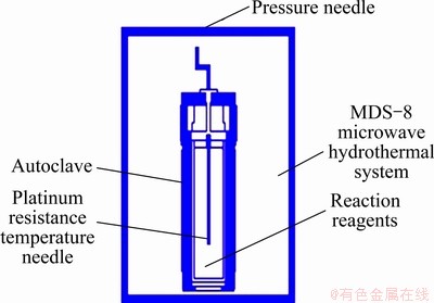
Fig. 1 Schematic diagram of preparation of CdS nano- crystallites by M-H in MDS-8 microwave hydrothermal system
3 Results and discussion
3.1 Phase composition
Figure 2 shows the XRD patterns of the as-prepared CdS powders with and without introduction of EDTA. Clearly, well crystallized CdS crystallites with wurtzite structure are obtained by the microwave hydrothermal process. All the diffraction peaks can be indexed as the hexagonal structure of CdS according to the standard diffraction card (JCPDS No. 41-1049). Sharp and strong diffraction peaks of the CdS powders are observed (Fig. 2(b)) without the adding of EDTA, which indicates the achieving of well crystallized CdS crystalline. But the weakened peak intensity and broadened diffraction peaks are obtained with the introduction of EDTA (Fig. 2(a)). This may result from the effect of nanoscale or nanostructure of the crystallites. By calculation, the size of the average nanoscale is about 30 nm according to the Scherrer equation.
Figure 3 shows the EDS spectrum collected from CdS crystalline prepared with EDTA. The EDS analysis reveals that the as-prepared CdS crystallites with addition of EDTA are composed of 50.65% Cd and 49.35% S (atomic fraction). No other element is detected, inferring the high purity of the as-prepared CdS crystallites.
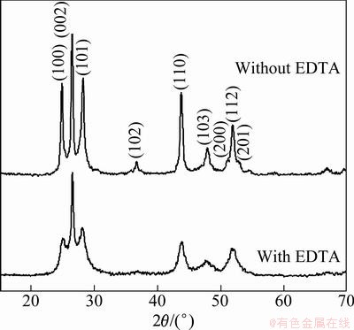
Fig. 2 XRD patterns of prepared CdS nanocrystallites
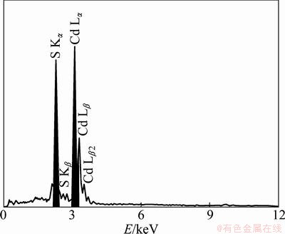
Fig. 3 EDS spectrum collected from CdS nanocrystallites prepared with EDTA
3.2 Morphology
The FE-SEM images of the CdS powders are shown in Fig. 4. Figure 4(a) shows that the as-prepared crystallites possess a flower-like morphology, composing of some small tetrahedron structures on the basis of certain rules. It can be clearly found that the CdS crystallites prepared by adding EDTA as a template are hollow spheres with a diameter range of 400-600 nm (Fig. 4(b)). The details of the hollow spherical structure can be clearly observed in Figs. 4(c), (d) and (e) with the high-magnification FE-SEM images. CdS hollow spheres with hierarchical structure are self- assembled by spherical nanoparticles of 30 nm, which is well consistent with the XRD results (Fig. 2(a)). These nanoparticles are in close contact with each other, forming small spherical structure, and then, the small balls come together to become more integrated and bigger hollow spheres, which can be seen from the images Figs. 4(c), (d) and (e). In addition, Fig. 4 demonstrates that the EDTA plays a vital role on the formation of CdS hierarchical hollow spheres.
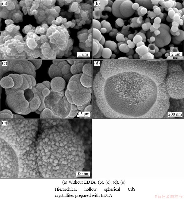
Fig. 4 FESEM images of as-prepared powders

Fig. 5 TEM images of as-prepared powders
Figure 5 shows typical TEM images of the prepared CdS hierarchical hollow spheres. The image in Fig. 5(a) shows the hollow structure of the as-prepared CdS. A low-magnification TEM image of one part of a CdS hierarchical hollow sphere is shown in Fig. 5(b). The hierarchical structure can be clearly observed. It is evident that the hollow sphere consists of many small nanoparticles (approximately 30 nm). HRTEM image of one nanoparticle of the CdS hierarchical hollow sphere shown in Fig. 5(c) reveals that the spacing of the crystallographic planes is about 0.676 nm, which is indexed as the (0001) plane of hexagonal CdS and is well consistent with the XRD result shown in Fig. 2.
3.3 Optical property
Figure 6(a) presents the UV-Vis absorption spectrum of the hierarchical hollow spherical CdS nanostructures with the absorption edge at about 468 nm. The optical band gap energy Eg was calculated by the equation: αhv=A(hv-Eg)1/2, where Eg is the optical band gap and A is a constant. Figure 6(b) shows the plot of (αhv)2vs. hv for the hierarchical hollow spherical CdS nanostructures. The band gap value of the hierarchical hollow spherical CdS nanostructures can be determined as 2.66 eV by extrapolation of the linear portion of the plot onto the energy axis. It is indicative of a blue shift about 0.24 eV compared with the band gap of bulk CdS (2.42 eV at room temperature). It is suggested that the blue shift of the absorption edge is attributed to the special morphology of the hierarchical structure. Moreover, a few point defects such as S vacancies due to the nonstoichiometric ratio of the as-produced CdS hierarchical hollow sphere (atomic ratio between Cd and S is about 1.03) also may lead to the blue shift of UV-Vis absorption spectrum.
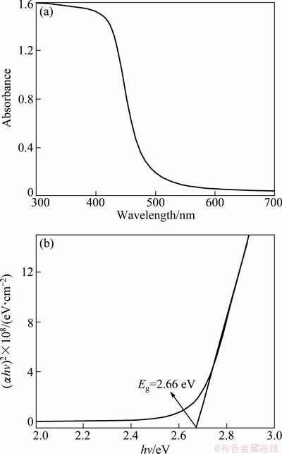
Fig. 6 UV-Vis spectrum (a) and relationship between (αhv)2 and hv (b) of hierarchical hollow spherical CdS
3.4 Effect of microwave and possible growth mechanism
The M-H process is an innovation of the conventional hydrothermal process by introducing microwave into the reaction [20]. Microwave heating offers many advantages over conventional autoclave heating, including rapid heating, homogeneous nucleation, and fast supersaturation by the rapid dissolution of precipitated hydroxides, which leads to a lower crystallization temperature and shorter crystallization time. Such behavior is presumably helpful to the formation of hierarchical hollow spherical CdS nanocrystals.
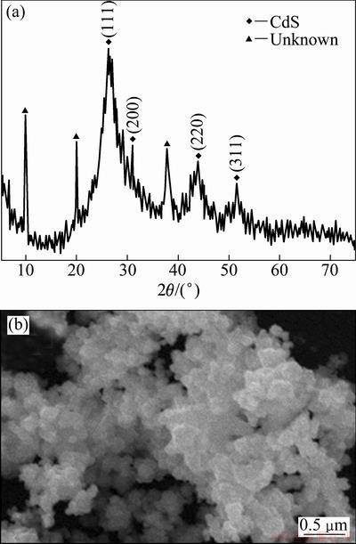
Fig. 7 XRD pattern (a) and SEM image (b) of CdS obtained at the same hydrothermal condition without microwave irradiation compared to Fig. 2(a)
The experimental phenomena support the above hypothesis. Figure 7 shows the XRD pattern and SEM image of the sample obtained under the same hydrothermal conditions compared to Fig. 2(a) but without microwave irradiation. The intensity and shape of the diffraction peaks in Fig. 7(a) indicate that the sample is not perfectly crystallized. Some peaks attributable to unknown impurity are observed. The diffraction peaks can be indexed as the zinc blende structure of CdS according to the standard diffraction card (JCPDS No.65―2887). The SEM image (Fig. 7(b)) of the as-prepared CdS crystals shows an irregular morphology, which is consistent with the XRD result. Hexagonal wurtzite structure is the high-temperature variant of the cubic zinc blende structure, which demonstrates that M-H process accelerates the reaction and leads to the growth and crystallization of CdS in a shorter time and lower temperature. In a word, the role of microwave is not only to accelerate the reaction but also to lead to the growth and crystallization of CdS with special morphology. In our research, Cd2+ and S2- are provided by hydrolysis of CdCl2・H2O and Na2S2O3・5H2O, respectively. Therefore, the mechanism of the formation of CdS hierarchical hollow spheres under the synergies of microwave irradiation and EDTA is proposed as follows:
1) The microwave irradiation will quicken the hydrolysis process and then accelerate the nucleation rate of CdS, leading to the enormous formation of the small primary CdS nanoparticles.
2) The freshly formed nanoparticles will spontaneously land on the previous CdS nanoparticles, and under the EDTA effect, CdS hierarchical hollow spheres can be formed by self-assembled growth.
3) Small CdS hierarchical hollow spheres may aggregate in an oriented fashion to produce a larger hollow sphere, as shown in Fig. 4(c).
Although the exact formation mechanism for this special nanostructure is not yet exactly clear, it is believed that the growth of the complex nanostructures is both microwave-assisted and template-directed.
4 Conclusions
1) CdS hierarchical hollow spheres with wurtzite structure have been synthesized with EDTA as a template by microwave hydrothermal process.
2) The XRD patterns and EDS spectrum demonstrate that the products are well crystallized with high purity. SEM and TEM images show that the hierarchical hollow spherical CdS nanostructures with a diameter range of 400-600 nm are self-assembled by nanoparticles of 30 nm. The blue shift of the absorption edge is found to be relevant to the special morphology which consists hierarchical hollow spherical CdS nanostructure and the S vacancies.
3) EDTA and microwave irradiation play an important role on the preparation of the CdS hierarchical hollow spheres. More experiments will be done to discuss the catalytic effect of the CdS hierarchical hollow spheres on the photo-catalytic reduction of CO2.
References
[1] SCHLAMP M C, PENG X G, ALIVISATOS A P. Improved efficiencies in light emitting diodes made with CdSe(CdS) core/shell type nanocrystals and a semiconducting polymer [J]. Journal of Applied Physics, 1997, 82: 5837-5842.
[2] DUAN X F, HUANG Y, AGARWAL R, LIEBER C M. Single-nanowire electrically driven lasers [J]. Nature, 2003, 421(6920): 241-245.
[3] CHEMSEDDINE A, JUNGBLUT H, BOULMAAZ S. Investigation of the nnocluster self-assembly process by scanning tunneling microscopyand optical spectroscopy [J]. J Phys Chem, 1996, 100: 12546-12551.
[4] GU Li. Fabrication of 2D and 3D dendritic nanoarchitectures of CdS [J]. Transactions of Nonferrous Metals Society of China, 2008, 18: 904-907.
[5] TRINDADE T, O’BRIEN P, PICKETT N L. Nanocrystalline semiconductors: synthesis, properties, and perspectives [J]. Chem Mater, 2001, 13: 3843-3858.
[6] AMALNERKAR D P. Photoconducting and allied properties of CdS thick flms [J]. Materials Chemistry and Physics, 1999, 60: 1-21.
[7] LIU Jin-ku, LUO Chong-xiao, YANG Xiao-hong, ZHANG Xiao-yu. Ultrasonic-template method synthesis of CdS hollow nanoparticle chains [J]. Materials Letters, 2009, 63: 124-126.
[8] ZHU Jun-jie, XU Shu, WANG Hui, ZHU Jian-min, CHEN Hong-yuan. Sonochemical synthesis of CdSe hollow spherical assembies via an in-situ template route [J]. Advance Materials, 2003, 15(2): 156-159.
[9] CHEN Shu-tang, ZHANG Xiao-ling, ZHANG Qiu-hua, TAN Wei-hong. Trioctylphosphine as both solvent and stabilizer to synthesize CdS nanorods [J]. Nanoscale Research Letters, 2009, 4: 1159-1165.
[10] ZHANG Hui, YANG De-ren, MA Xiang-yang, XUE Duan-lin. Some critical factors in the synthesis of CdS nanorods by hydrothermal process [J]. Materials Letters, 2005, 59: 3037-3041.
[11] XU Dong-sheng, XU Ya-jie, CHEN Da-peng, GUO Guo-lin, GUI Lin-lin, TANG You-qi. Preparation of CdS single-crystal nanowires by electrochemically induced deposition [J]. Advance Materials, 2000, 12(7): 520-522.
[12] CHEN Ming, PAN Li-jia, GAO Jie-ming, JI Hong-mei, JI Guang-bin, MA Xian-jia, ZHENG You-dou. Synthesis of CdS nanoplates by PAA-assisted hydrothermal approach [J]. Materials Letters, 2006, 60: 3842-3845.
[13] WANG Li-cheng, CHEN Lu-yang, LUO Tao, QIAN Yi-tai. A hydrothermal method to prepare the spherical ZnS and flower-like CdS microcrystallites [J]. Materials Letters, 2006, 60: 3627-3630.
[14] HE Xiao-bo, GAO Lian. CdS hierarchical spindles: Structural defects and properties [J]. Materials Letters, 2009, 63: 995-997.
[15] PAN Qing-tao, HUANG Kai, NI Shi-bing, WANG Qi, YANG Feng, HE De-yan. Fabrication and photoluminescence properties of large-scale hierarchical CdS dendrites [J]. Materials Letters, 2007, 61: 4773-4776.
[16] ZHANG Peng, GAO Lian. Synthesis and formation mechanism of CdS nanorods via hydrothermal microemulsion [J]. Journal of Inorganic Materials, 2003, 18(4): 772-776.
[17] HU Bao-yun, HUANG Jian-feng, CAO Li-yun, WU Jian-peng, ZHANG Qin-feng. Preparation of CdS sphere-like microcrystals by microwave hydrothermal process [J]. Journal of Chinese Ceramic Society, 2010, 38(5): 850-853. (in Chinese)
[18] HU Bao-yun, HUANG Jian-feng, ZHANG Hai, CAO Li-yun ZHANG Qin-feng, WU Jian-peng. Influence of S/Cd molar ratio on the morphology and optical property of CdS microcrystalline prepared by microwave hydrothermal [J]. Chinese Journal Inorganic Chemistry, 2010, 26(6): 1039-1043. (in Chinese)
[19] HUANG Jian-feng, XIA Chang-kui, CAO Li-yun, ZENG Xie-rong. Facile microwave hydrothermal synthesis of zinc oxide one-dimensional nanostructure with three-dimensional morphology [J]. Materials Science and Engineering B, 2008, 150: 187-193.
[20] KOMARNENI S, ROY R, LI Q H. Microwave-hydrothermal synthesis of ceramic powders [J]. Materials Research Bulletin, 1992, 27: 1393-1405.
微波水热法制备分等级空心球状CdS纳米结构
胡宝云1,景镇子1,黄剑锋2,恽 俊3
1. 同济大学 材料科学与工程学院,上海 201804;
2. 陕西科技大学 教育部轻化工助剂化学与技术重点实验室,西安 710021;
3. 上海交通大学 环境科学与工程学院,上海 200240
摘 要:以氯化镉和硫代硫酸钠为原料,以乙二胺四乙酸(EDTA)为模板剂,采用微波水热(M-H)法成功制备了空心球状CdS纳米结构。采用X射线衍射仪(XRD)、场发射扫描电子显微镜(FE-SEM)、能量弥散X射线谱(EDS)和高分辨透射电子显微镜(HRTEM)对所制备的CdS纳米结构进行表征。采用紫外-可见吸收光谱研究所制备的分等级空心球状CdS纳米结构的光学性能。结果表明:得到的CdS是具有纤锌矿结构的直径为400~600 nm的分等级空心球状纳米结构,这种结构由30 nm左右的纳米颗粒自组装构成。EDTA和微波辐射在分等级空心球状CdS纳米结构的形成过程中起了重要作用,讨论了这种作用并提出可能的生长机理。所制备的分等级空心球状CdS纳米结构具有较好的蓝光发射性能。
关键词:CdS;微波水热法;分等级空心球状结构;光学性能
(Edited by HE Yun-bin)
Foundation item: Project (50942047) supported by the National Natural Science Foundation of China; Project (NCET-06-0893) supported by the Foundation of New Century Excellent Talent in University of China
Corresponding author: JING Zhen-zi; Tel/Fax: +86-21-65908420; E-mail: zzjing@tongji.edu.cn