Article ID: 1003-6326(2005)02-0410-04
Effect of annealing treatment on optical and electrical properties of ZnO films
WANG Wan-lu(����¼), LIAO Ke-jun(�ο˿�), LI Li(�� ��),
WU Zhi-hua(���ӻ�), WANG Yong-tian(������), ZHANG Jin(�� ��)
(Department of Applied Physics, Chongqing University, Chongqing 400044, China)
Abstract: The ZnO-Al films were prepared by R.F. magnetron sputtering system using a Zn-Al target (with purity of 99.99%). The obtained films were characterized by X-ray diffraction, SEM and optical and electrical measurements. The experimental results show that the properties of ZnO films can be further improved by annealing treatment. The crystallinity of ZnO films becomes better, and the optical gap energy is decreased, but thermoelectric power is enhanced after heat treatment. The optical gap energy decreases from 3.75eV to 3.68eV when the annealing temperature increases from 25�� to 400��.This can be ascribed to the decrease of carrier concentration, resulting in Burstein shift.
Key words: ZnO films; annealing treatment; Seebeck effect; optical gap energy CLC number: O643
Document code: A
1 INTRODUCTION
ZnO is a ��-�� compound semiconductor with a wide direct band gap and a hexagonal wurtzite structure (space group p63mc with cell parameters a=0.3249nm, c=0.5206nm). Owing to their unique physical and chemical properties, ZnO thin films can be used as surface acoustic wave devices and bulk acoustic resonators, transparent electrodes, gas and optical sensors, ultrasonic oscillators, transducers, optical wave guides, photoprotective coatings, ultraviolet laser, light-emitting diodes and light diodes[1-7]. ZnO films have widely been studied by many research groups from synthesis techniques to actual applications. At present, ZnO films can be synthesized by various methods such as DC and RF magnetron sputtering[8], PLD[9], CVD[10], SS-CVD[11], spray pyrolysis[12], sol-gel[13]. P- and N-type doping ZnO films have also gained great progress[14, 15]. However, some fundamental issues need to be further studied in order to obtain high quality ZnO thin films. In this work, effect of the annealing treatment on the optical and electrical properties of ZnO films was investigated. The experimental results show that the annealing treatment has an important influence on the structures and optical gap energy, and thermoelectric power of ZnO thin films.The results are very important for the quality and applications of ZnO films.
2 EXPERIMENTAL
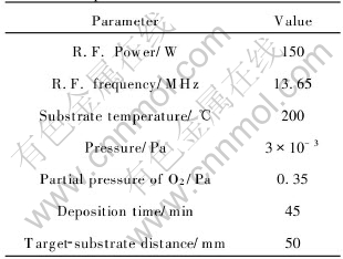
ZnO thin films were prepared by R.F. Magnetron sputtering system using a Zn target(99.99%) containing Al of 1.5% in Zn with diameter of 7.62cm and thickness of 5mm. Soda lime glass was used as the substrates. The substrate materials were thoroughly cleaned with organic solvents and dried before loading in the deposition chamber. The reactive chamber was first pumped down to about 1.33332��10-6Pa using molecular pump, and a sputter-etch of 5min was removed the target surface contamination. After that, a mixture of argon and oxygen was introduced, and the ratio of argon to oxygen was controlled by two electronic flow controllers. The substrate temperature was monitored using a thermo-cooper attached near the substrate. The deposition conditions were shown in Table 1.
Table 1 Deposition conditions of ZnO films
The ZnO films obtained were characterized by scanning electron microscopy, X-ray diffraction and optical and electrical measurements. SEM image of ZnO films is shown in Fig.1. The ZnO particle size is about 100-200nm, which depends on the deposition conditions.
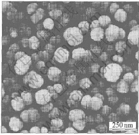
Fig.1 SEM image of ZnO films
3 RESULTS AND DISCUSSION
ZnO films with 600nm in thickness containing 1.5%Al concentration at room temperature were annealed in Ar atmosphere at temperature ranging from 25�� to 400��. The heated rate of samples was about 10��/min, and time duration was 2h. The experimental results indicate that the annealing treatment causes the X-ray diffraction peak to shift toward a high value as shown in Fig.2. The peaks move from 2��=34.7�� to 2��=35.2�� when the annealing temperature increases from 25�� to 400�� as shown in Fig.3. This is because of Al doping into ZnO films, resulting in a reduced lattice constant and internal stress degradation after heat treatment. On other hand, the crystallite size of ZnO also increases with annealing temperature increasing. The particle size increases from 100nm to 125nm when the annealing temperature increases from 25�� to 400��. From Fig.2, it can be seen that the ZnO thin films show preferred orientation of (002) plane with hexagonal structure (wurtzite type).
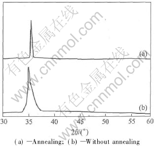
Fig.2 Effect of annealing treatment on XRD patterns graphs of ZnO films

Fig.3 Changes of XRD peak with annealing temperature
The optical properties of ZnO films can be obtained the by analyzingUV-Visible spectra. The film transmittance is given by the following formula[16]:

where �� is optical absorption coefficient,
R1=[(ns-1)/(ns+1)]2,
R2=[(nf-ns)/(nf+ns)]2,
R3=[(nf-1)/(nf+1)]2,
��=4��nf/��,
ns and nf are the refractive index of substrate and films, respectively, t and �� are film thickness and wavelength. nf can be obtained by

where ��1 and ��2 are the wavelength corresponding to the i-th and (i+1) extreme of the T-�� curve. From Eqns.(1) and (2), absorption coefficient �� is determined. The change of �� with photon energy (hv) obeys the relation by
(��hv)2=B(hv-Eopt)(3)
where B is a constant and Eopt the optical gap energy. The Eopt values are gained by extrapolating the linear portion of the plots of (2hv)2 vs hv to ��. Fig.4 shows optical gap energy as a function of the annealing temperature for ZnO films (1.5%Al). The optical gap energy decreases from 3.75eV to 3.68eV with annealing temperature increasing from 25�� to 400��.
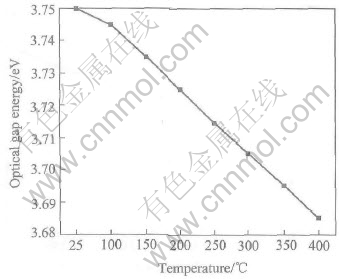
Fig.4 Optical gap energy as function of annealing temperature for ZnO films
The thermoelectric power of ZnO films was measured in the temperature range from 25�� to 200��. Two copper-constantan thermocouples closely attached to the ends of a sample were used as measurement of both temperature difference ��T and the thermal electromotive force in the films-copper circuit.
The reference points of the thermocouples were electrically insulated and put in an ice water bath. Typical plots of the thermoelectric power for ZnO films are shown in Fig.5. It is very apparent that the annealing treatment could enhance Seebeck effect in the ZnO films.
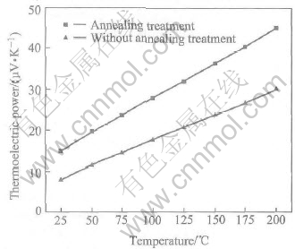
Fig.5 Relationship between thermoelectric power and temperature for ZnO films
Like the experimental results mentioned above, the annealing treatment has an important influence on the optical and electrical properties of ZnO films. If one assumes spherical energy surface for the crystalline ZnO films, and that only the conduction band high curvature, then[17, 18]
n=8��/3h3(m*e��E)3/2(4)
where n is the free carrier concentration on the conduction band, ��E is the Burstein shift (namely ��E=Eopt-Eg)[17], and m*e is the effective mass of conduction electron. The carrier concentration decreases and the resistivity increases after annealing treatment[19], which causes ��E to increase. Also the optical gap energy Eopt further decreases after heat treatment.
4 CONCLUSIONS
Al-doped ZnO films were prepared by R.F. magnetron sputtering. The experimental results show that the annealing treatment has a significant effect on the structure and properties of ZnO thin films. This is due to the decrease of carrier concentration after annealing treatment, resulting in Burstein shift. These results are very important for studying the quality and applications of ZnO films.
REFERENCES
[1]Water W, CHU Sheng-yuan. Physical and structural properties of ZnO sputtered films [J]. Mater Lett, 2002, 55: 67-72.
[2]Takayuki S, Kazuya U, Eiji M, et al. Characterization of sputtered ZnO thin films as sensors and actuator for diamond AFM probe [J]. Sensors and Actuators A, 2002, 102: 106-113.
[3]Michio K, Toshinori M, Makoto M, Piezoelectric and optical properties of ZnO films deposited by an electron-cyclotron-resonance sputtering system [J]. J Cryst Growth, 2002, 237-239: 523-527.
[4]Kalantar Z.K, Adrian T, Wojtek W, et al. A novel love-mode device based on a ZnO/ST-cut quartz crystal structure for sensing applications [J]. Sensors and Actuators A, 2002, 100: 15-143.
[5]Emanetoglu N W, ZHU Jun, CHEN Ying, et al. Surface acoustic wave ultraviolet photodetectors using epitaxial ZnO multilayers grown on r-plane sapphire [J]. Appl Phys Lett, 2004, 85: 3702-3705.
[6]Fortunato Elvira M C, Barquinha Pedro M C, Ana C M B G, et al. Wide-bandgap high-mobility ZnO thin-film transistors produced at room temperature [J]. Appl Phys Lett, 2004, 85: 2541-2544.
[7]KANG Hong-seong, KANG Jeong-seok, PANG Seong-sik, et al. Variation of light emitting properties of ZnO thin films depending on post-annealing temperature [J]. Mater Sci and Eng B, 2003, 102: 313-316.
[8]LI Zheng-wei, GAO W. ZnO thin films with DC and RF sputtering [J]. Mater Lett, 2004, 58: 1363-1370.
[9]Yoshiki N, Tatsuo O, Mitsuo M. Deposition of ZnO film by pulsed laser deposition at room temperature [J]. Appl Surf Sci, 2002, 197-198: 368-370.
[10]Kazuhiko K, Kouji O, Naoyuki T, et al. Epitaxial growth of ZnO thin films exhibiting room- temperature ultraviolet emission by atmospheric pressure chemical vapor deposition [J]. Thin Solid Films, 2002, 1: 116-119.
[11]LU Jian-guo, YE Zhi-zhen, HUANG Jing-yun, et al. Synthesis and properties of ZnO films with (100) orientation by SS-CVD [J]. Appl Surf Sci, 2003, 207: 295-299.
[12]Bougrine A, EI Hichou A, Addou M, et al. Structural, optical and cathodoluminescence characteristics of undoped and tin-doped thin films prepared by spray pyrolysis [J]. Mater Chem and Phys, 2003, 80: 438-445.
[13]Lee Jin-Hong, Ko Kyung-Hee, Park Byung-Ok. Electrical and optical properties of ZnO transparent conducting films by the sol-gel method [J]. J Cryst Growth, 2003, 247: 119-125.
[14]BIAN J M, LI X M, ZHANG C Y, et al. P-type ZnO films by monodoping of nitrogen and ZnO-based p-n homojunctions [J]. Appl Phys Lett, 2004, 85: 4070-4073.
[15]Kim Jae-Hyun, Kim Hyo-Jin, KIM Do-Jin, et al. Optical and magnetic properties of laser-deposited Co-doped ZnO thin films [J]. Solid State Commun, 2004, 131: 677-680.
[16]WANG Wan-lu, LIAO Ke-jun, LIU Gao-bin, et al. Influence of annealing treatment on the optical properties and structure of Cd2SnO4 thin films [J]. Surf Coat Techn, 2003, 167: 284-287.
[17]PENG Dong-liang, JIANG Sheng-rui, WANG Wan-lu. Effect of heat treatment on electrical and optical properties of Cd2SnO4 films [J]. Chin Phys Lett, 1993, 10: 189-192.
[18]Shan F K, Yu Y S. Band gap energy of pure and Al -doped ZnO thin films [J]. J Europ Ceram Soc, 2004, 24: 1869-1872.
[19]CHU Sheng-Yuan, Water W, Liaw Jih-Tsang. Influence of postdeposition annealing on the properties of ZnO films prepared by RF magnetron sputtering [J]. J Europ Ceram Soc, 2003, 23: 1593-1598.
Received date: 2004-12-01; Accepted date: 2005-01-18
Correspondence: WANG Wan-lu, Professor; Tel: +86-23-65103490; E-mail: wanluw@cqu.edu.cn
(Edited by HE Xue-feng)