
Effects of two-step annealing on properties of Cd1-xZnxTe single crystals
YANG Ge(杨 戈)1, JIE Wan-qi(介万奇)1, ZHANG Qun-ying(张群英)2,
WANG Tao(王 涛)1, LI Qiang(李 强)1, HUA Hui(华 慧)1
1. College of Materials Science and Engineering, Northwestern Polytechnical University, Xi’an 710072, China;
2. Beijing Power Machinery Research Institute, Beijing 100074, China
Received 10 April 2006; accepted 25 April 2006
Abstract: The Cd1-xZnxTe(CZT) single crystals were annealed by a two-step method including a vapor-environment step and a liquid-environment step in sequence. The effects of annealing on the properties of CZT were analyzed in detail. IR transmission measurement results show that IR transmission of CZT is improved dramatically after annealing. X-ray rocking curves indicate that the annealing treatment ameliorates crystal quality obviously, which is ascribed to the release of residual stress and the reduction of point defects. Photoluminescence(PL) spectra reveal that the full width at half maximum(FWHM) of the donor-bound exciton (D0, X) peak is reduced obviously, and the free exciton emission is weakened after annealing. Meanwhile, the intensity of the donor-acceptor pair(DAP) peak decreases to a great degree, which implies that the impurities are removed from CZT wafers. In addition, the deep defect-related emission band Dcomplex disappears after annealing, which mean that Cd vacancies are well-compensated. The results confirm that the two-step annealing is an effective approach to improve the qualities of CZT single crystals.
Key words: Cd1-xZnxTe single crystal; impurities; defects; semiconducting II-VI materials
1 Introduction
The compound semiconductor Cd1-xZnxTe (CZT) has the promising potential applications for the high energy nuclear radiation detection[1-5]. However, high quality CZT single crystals are very difficult to obtain. As-grown CZT crystals by the most popular Bridgman method usually contain high density of defects, such as Cd vacancies, Te antisites and Te precipitates, which deteriorate the optoelectronic properties of CZT crystals seriously. Therefore, some measures must be adopted to eliminate the effects of these defects. Several groups reported that, the annealing treatment is an effective approach to depress defects in CZT[2-4]. However, the corresponding mechanisms are still not well understood until now. The further investigations of annealing treatment are necessary to achieve good quality CZT crystals.
In this research, we attempted to anneal CZT wafers by a two-step method including a vapor- environment step and a liquid-environment step in sequence. The effects brought by the annealing were analyzed according to IR transmission spectra, X-ray rocking curves and PL spectra.
2 Experimental
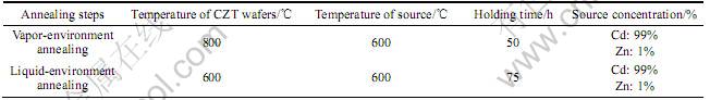
A CZT crystal was grown with the modified Bridgman(MB) method. High purity raw materials of Cd (7N), Zn (7N) and Te (7N) were used to prevent the unintended impurities. The mole ratio of Cd, Zn and Te was 0.9∶0.1∶1.0. The ingot was cut along (111) face with the dimension of 10 mm×10 mm×20 mm. Before annealing, all wafers were mechanically polished with MgO suspension carefully, and then, chemically polished with 5% bromine in methanol (Br-MeOH) for 4 min. Source metals, Cd(7N) and Zn(7N), with a specified mass proportion, were sealed by CZT wafers in a quartz ampoule under the vacuum of 0.1 mPa. Annealing experiments were carried out in a two-zone furnace. As the first step, CZT wafers were annealed in CdZn vapors for a period. Then, the wafers were immersed in CdZn melt alloy for the liquid-environment annealing. The annealing parameters are listed in Table 1. After annealing, all wafers were mechanically and chemically polished to remove the surface damaged layer.
IR transmission tests were carried out at room temperature by a Nicolet Nexus 670 spectrometer. X-ray rocking curves were measured with a PANalytical X'Pert Pro diffractometer. In the photoluminescence (PL) measurements, the samples were attached on a cold copper finger in a closed-cycle cryostat with grease to keep the sample temperature at 10 K. An argon ion laser with the wavelength of 488 nm was used to excite the PL spectrum. A Triax 550 tri-grating monochromator with a photo-multiplier tube(PMT) was employed to collect and analyze the signals emitted from the samples.
3 Results and discussion
3.1 IR transmission spectrum
IR transmission spectrum is an important means to evaluate the quality of CZT crystals. As shown in Fig.1, the IR transmission curves of as-grown CZT are a straight line with the average transmission of about 45%. However, the transmission increases to about 63% after annealing. The phenomenon can be explained according to absorption behaviors in the crystals. The transmission of CZT can be expressed by [5]
 (1)
(1)
where R is the reflectivity; d is the sample thickness, and α is the absorption coefficient. For the CZT sample, the thickness d is 2mm and the reflectivity R is 0.21[6]. The absorption coefficient, α, is mainly influenced by the following factors: 1) free carrier absorption; 2) precipitates scattering; 3) impurity absorption. In the wavenumber domain of 1 000 cm-1 to 4 000 cm-1 investigated in this work, α is dominated by the free carrier absorption and precipitates scattering. Impurity absorption only takes effect at low temperature. After annealing, Te precipitates were reduced to a large degree [7], therefore, the transmission loss by precipitates scattering was decreased. In addition, the effect of free carrier absorption on the absorption coefficient α can be
expressed by the following equation [8]
 (2)
(2)
where N is the concentration of free carrier; λ is the wavelength of IR emission; m is the effective mass of a free carrier, n is the refractive index; τ is the relaxation time. The liquid-environment annealing in step 2 is helpful to remove the impurities, such as In, Li and Na from the wafers[7]. As we know, these impurity atoms can ionize and provide free electrons in CZT. During the annealing, In, Li and Na atoms migrated to the surface layer of wafers, which were taken away by the following polishing. Therefore, the impurities of In, Li and Na in the inner CZT bulk crystal was reduced remarkably, which resulted in the decrease of the concentration of free carrier. Judging from Eqn.(2), the change of the concentration of free carrier brought on the fall of absorption coefficient. According to Eqn.(1), reducing absorption coefficient increased the IR transmission of annealed CZT.

Fig.1 IR transmission spectra of as-grown and annealed CZT wafers.
3.2 X-ray rocking curves
X-ray rocking curves of CZT wafers before and after annealing are shown in Fig.2. Several interesting phenomena are found comparing the two curves. First, the full width at half maximum (FWHM) of X-ray rocking curve was reduced remarkably after annealing. The FWHM of as-grown CZT is 0.057?. Whereas, this
Table 1 Parameters of two-step annealing of CZT crystals
value is lowered to 0.027? for annealed CZT. Secondly, the rocking curve splits into two peaks before annealing, which can be separated with two fittings by Gaussian function. S1 peak locates at θ=38.413? and S2 peak locates at θ=38.454?. Wherein, S1 peak is the main peak, whose intensity is much higher than that of S2 peak. After annealing, the splitting of the peak disappears and the position of the peak shifts to θ=38.355?. These phenomena indicate that the crystal quality is improved after annealing.
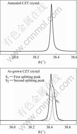
Fig.2 X-ray rocking curves of as-grown and annealed CZT single crystals
The annealing treatment provides a Cd/Zn-rich environment around the wafers. In this condition, Cd atoms diffuse into the wafers and compensate Cd vacancies effectively. At the same time, excess Te migrates from the inner of CZT wafers, hence, the amount of Te precipitates is decreased. The decrease of the FWHM of X-ray rocking curve is mainly due to the reduction of Cd vacancies and Te precipitates, which ameliorate crystal quality remarkably. In addition, there also exists some residual stress in as-grown CZT crystals, which results in the relaxation of crystal lattice. The annealing treatment could release the stress effectively and change the nature of crystal lattice. According to Ref.[1], the lattice constant a can be expressed as  . Hereby, the shift of θ in our experiment means that the lattice constant reduced after annealing. The splitting of the peak, in our opinion, is likely to be associated with the small angle grain boundaries determined by the dislocations in the CZT crystals. The annealing treatment adopted reduces the amount of dislocations and, therefore, lowers the density of small angle grain boundaries, which avoided the splitting of X-ray rocking curve.
3.3 Photoluminescence (PL) spectrum
The typical low temperature PL spectrum of CZT samples after the two-step annealing is shown in Fig.3. For reference, the PL spectrum of an as-grown CZT wafer is also presented. Both of the spectra can be divided into three regions: region (Ⅰ) (1.680-1.630 eV), the near band-edge region consists of free and bound exciton peak; region (Ⅱ) (1.630-1.575 eV), covering the donor-acceptor pair (D, A) recombination and its phonon replicas; region (Ⅲ) (1.575-1.430 eV), showing the defect-related region associated with some impurity-complex energy levels. Here, the band located in the defect-related region is named as Dcomplex peak. As shown in Fig.3, when CZT wafers are annealed, four interesting phenomena are found in the PL spectra. First, the full width at half maximum (FWHM) of the donor-bound exciton (D0, X) peak reduces obviously in the case of annealed CZT. Secondly, the intensity of the FE peak fell dramatically after annealing. Thirdly, a fine DAP structure and its longitudinal optical phonon replicas (DAP-LO) are distinct before annealing. However, both of them are weakened for the annealed CZT. Fourthly, there exists a Dcomplex band centered at 1.553 9 eV in the PL spectrum of as-grown CZT crystal. After annealing, this defect-related band disappears absolutely.
The FWHM of (D0, X) peak is an important indicator of crystal quality and the small FWHM implies the good crystal quality[9]. As analyzed the forth, the reduction of Te precipitates and Cd vacancies during the annealing improved the crystal quality of CZT, which resulted in the decrease of the FWHM of (D0, X) peak. According to Ref.[1], the band-gap energy Eg of CZT can be determined from the position of (D0, X) peak, which lies at 13 meV below Eg. The DAP peak centered at 1.611 5 meV was deduced to lie at 58 meV below the conduction band, Eg (-58 meV), which was consistent with the values for the effective mass acceptors of Li and Na in CdTe and CZT (Ea ≈ 56.8 meV) [10,11]. Therefore, the shallow acceptors in the DAP emission were ascribed to the impurities of Li and Na from the raw materials. In addition, the FE peak was possibly due to the dissociation of the excitons bound to the donor of Li and Na, which existed in the starting materials. During the
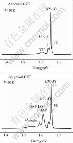
Fig.3 Photoluminescence(PL) spectra of as-grown and annealed CZT wafers
liquid-environment annealing, the impurities of Li and Na migrated from CZT wafers to the annealing medium. Hereby, the change of the intensities of DAP peak and FE peak could be attributed to the reduction of Li and Na through annealing treatment. This argument is also supported by the experimental results of LI et al[4]. As far as Dcomplex, it is generally accepted that a Cd vacancy-related complex, the so-called center A, was responsible for this peak[1]. In the Cd(Zn)-rich atmosphere established by the two-step annealing, Cd and Zn atoms diffused into the wafers and bonded with Te atoms. Therefore, the amount of Cd vacancy was reduced remarkably and, thus, that of center A was also decreased, which resulted in the decrease of the intensity of Dcomplex peak.
4 Conclusions
1) IR transmittance of CZT is improved drama- tically after annealing, which means that the annealing can reduce Te precipitates and remove the impurities from CZT wafers.
2) The FWHM of X-ray rocking curve decreases for the annealed CZT. Meanwhile, the splitting of the peak disappears after annealing, which indicates that the crystal quality of CZT is ameliorated effectively by annealing.
3) PL measurement reveals that the FWHM of (D0, X) peak and the intensity of FE peak are reduced obviously by annealing. A fine DAP structure and its longitudinal optical phonon replicas (DAP-LO) are distinct before annealing, both of which are weakened for the annealed CZT. In addition, the Dcomplex peak disappears absolutely after annealing, which confirms that the annealing can compensate Cd vacancies and remove the impurities from CZT wafers.
References
[1] SCHLESINGER T E, TONEY J E, YOON H, LEE E Y, BRUNETT B A, FRANKS L, JAMES R B. Cadmium zinc telluride and its use as a nuclear radiation detector material [J]. Mater Sci and Eng, 2001, 32: 105-189.
[2] LI Yu-jie, MA Guo-li, ZHANG Xiao-na, JIE Wan-qi. The annealing of Cd1-xZnxTe in CdZn vapors [J]. J Electron Mater, 2002, 31: 834-840.
[3] SEN S, LIANG C S, RHIGER D R, STANNARD J E. Reduction of CdZnTe substrate defects and relation to epitaxial HgCdTe quality [J]. J Electron Mater, 1996, 25: 1188-1195.
[4] LI Guo-qiang, JIE Wan-qi, WANG Tao, YANG Ge. Impurities in CdZnTe crystal grown by vertical bridgman method [J]. Nucl Instr and Meth A, 2004, 534: 511-517.
[5] SEN S, RHIGER D R, CURTIS C R, KALISHER N H, HETTICH H L, CURRIE M C. Infrared absorption behavior in CdZnTe substrates [J]. J Electron Mater, 2001, 30: 611-618.
[6] ZHU Ji-qian, CHU Jun-hao, ZHANG Xiao-ping, LI Biao, CHENG Ji-jian. Study on crystalline quality of Cd-annealing CdZnTe wafers grown by Bridgman method [J]. Chinese Journal of Semiconductors, 1997, 18: 782-786.(in Chinese)
[7] LI Yu-jie. Investigation of the Defects in Cd1-xZnxTe Crystals and the Heat Treatment of Wafers [D]. Xi’an: Northwestern Polytechnical University, 2002.
[8] ZONG Xiang-fu, WONG Yu-min. The Foundations of Material Physics [M]. Shanghai: Fudan University Press. 2001. (in Chinese)
[9] TSENG P Y, FU C B, KUO M C, YANG C S, HUANG C C, CHOU W C, SHIH Y T, HSIN H Y, LAN S M, LAN W H. Optical properties of Cd1-xZnxTe crystals grown by temperature gradient solution growth [J]. Mater Chem and Phys, 2002, 78: 529-533.
[10] MOLVA E, PAUTRAT J L, SAMINADAYAR K, MILCHBERG G, MAGNEA N. Acceptor states in CdTe and comparison with ZnTe, general trends [J]. Phys Rev B, 1984, 30: 3344-3354.
[11] HOSCHL P, IVANOV Y M, BELAS E, FRANC J, RILL R G, HLIDEK P, MORAVEC P, ZVARA M, SITTER H, TOTH A L. Electrical and luminescence properties of (CdZn)Te single crystals prepared by the vertical gradient freezing method[J]. J Cryst Growth, 1998, 184/185: 1039-1043.
(Eidted by LI Yan-hong)
Foundation item: Project(50336040) supported by the National Natural Science Foundation of China
Corresponding author: YANG Ge; Tel: +86-29-88486065; Fax: +86-29-88495414; E-mail: yangge6886@hotmail.com

