J. Cent. South Univ. (2017) 24: 270-275
DOI: 10.1007/s11171-017-3427-2

First-principle study of electronic structure and optical properties of Au-doped VO2
HUANG De-wei(�Ƶ�ΰ)1, ZHAO Cui-hua(�Դ仪)1, CHEN Jian-hua(�½���)2,
LI Yu-qiong(������)2, LI Wei-zhou(���)1
1. College of Materials Science and Engineering, Guangxi University, Nanning 530004, China;
2. Guangxi Colleges and University Key Laboratory of Minerals Engineering, Guangxi University,Nanning 530004, China
 Central South University Press and Springer-Verlag Berlin Heidelberg 2017
Abstract: The electronic structure and optical properties of VO2 and Au-VO2 were studied using density functional theory. The calculation results show that the interaction between Au and O is stronger than that between V and O. There exists not only the covalent bonding but also ionic bonding in Au��O bond. The band gap of Au-VO2 is smaller than that of VO2, while the dielectric constant, conductivity, and intensity of optical absorption of Au-VO2 are larger than those of VO2.
Key words: Au-VO2; electronic structure; optical property; First-principle
1 Introduction
Vanadium dioxide is the most amazing technologically thermochromic material because of the reversible metal-to-insulator transition (MIT). The crystalline phases will be quite different when the temperature changes. It is the monoclinic phase (M1) and infrared-transmitting semiconductor or narrow gap insulator at a low temperature, which transforms to the infrared-reflecting tetragonal rutile structure phase (R) at a critical temperature near 340 K [1�C5]. It becomes metallic state conductor above the TMIT (metal�Cinsulator transition temperature). There is another intermediate phase between the monoclinic phase (M1) and rutile (R), which is the insulator monoclinic phase (M2) [6]. The transition takes place in the arrangement of the atomic structure and the properties like optical and electronic [7], and on the time scale of 10-7�C10-5 s for nano-scale devices [8]. The V atoms of the M1-VO2 are the formation of Zig-zag chain V�CV along the Cb axis, but there are two formations in the M2-VO2 along the Cb axis. One is the V atomic chains in pairs but does not tilt (relative to the Cb axis), another is the V atomic chains in tilt but is not in pairs [9]. These fascinating characteristics make VO2 a further application in thermodynamic window coating, smart optoelectronic switcher, memory material, actuators, photonics technologies, and diffractive elements, and so on [10�C13]. However, some drawbacks in properties and practical applications need to be resolved, such as high critical temperature, low visible transparency, and limited solar-energy modulation efficiency [14]. The last two are calculated by
 (1)
(1)
where ��lum represents the spectral sensitivity of the light�Cadapted eye; ��sol represents the solar irradiance spectrum for an air mass of 1.5 corresponding to the position 37�� above the horizon [14]. It must have been a widely application in our life when these drawbacks are overcome, especially the critical temperature near to room temperature (298 K). Phase transition temperature can be affected by temperature, stress, doping, nonstoichiometry, graining, or a combination of all factors. The studies have shown that some characteristics have different change when some higher-valence ions (Nb5+, Mo5+, W6+) were doped to the VO2 [15], such as the crystalline structure, color, Mott phase transition, optical properties, and electrical properties, and the TMIT can be reduced. On the contrary, the TMIT can be increased when low-valence ions (Al3+, Cr3+, Ga3+) were doped. Therefore, doping can decrease or increase the phase transition temperature and increase the visible transparency [16, 17]. The studies also showed that W is one of the best effective dopant to decrease the transition phase temperature at a certain content, and the decrease of phase transition temperature will keep the linear relationship with the doping contents performance, which could be interpreted by Peierls-like phase transition, but it is an irreversible process [18]. LI et al [19] showed that purely Mg-doped can increase the bandgap ((3.9��0.5) eV) per unit of atom ratio Mg/(Mg+V). Doped VO2 exhibits different characteristics when some nonmetal elements like F, Cl, Br and I were doped to VO2 compared to metal elements. For instance, the phase transition temperature of the F-doped VO2 is 308 K at 2.93% F in VO2. The halogen-doped VO2 can decrease the bandgap, which is different from Mg-doped widening the bandgap. Cl-doped VO2 at V is the best one to achieve good VO2 thermochromic energy-saving material [20, 21]. The glass cover with F-doped VO2 not only increases the solar-heat shielding ability but also modifies a comfortable color, which still keeps excellent solar modulation abilities and a suitable visible transmittance. It had been demonstrated that the phase transition temperature will decrease when oxygen vacancy is introduced into the VO2 thin film [22].
The underlying mechanism of the MIT in VO2 is considered the Mott-Hubbard-like driven by electron- electron correlation or Peierls-like driven by electron- phonon interactions, which continues debating. However, a lot of research had shown that doping is the effective way to change the band gap and trigger the phase structure change. Au is the most conductivity metal element. KIM et al [23] studied the conductance control in VO2 nanowires by physical vapor deposition. The results demonstrated that Au-doped VO2 has good conductance control. In this work, electronic structures and optical properties of pure VO2 and Au-doped VO2 were studied using the first-principle calculations, including energy gap, density of states, Mulliken population, dielectric function, conductivity and optical absorption. The emphasis was put on the mechanism of the electronic structures and optical properties changes of VO2 caused by Au doping.
2 Computational methods and models
2.1 Computational methods
The electronic structures and optical properties of pure VO2 and Au-doped VO2 were studied using the periodic DFT calculations implemented in the CASTEP code, using the generalized-gradient-approximations (GGA) in the form of the Perdew�CWang 91 (PW91) exchange-correlation functional. A simplified version of the rotationally invariant LDA+U method was used, where the adopted values of U in the LDA +U were set at 2.5 eV for the vanadium d electrons. Calculations were performed as nonmagnetic. The energy cutoff was set at 340 eV, and a 1��1��1 uniform Monkhorst-Pack k-point grid was used for M1 phase. The convergence tolerances for geometry optimization calculations were set to the maximum energy change of 2��10�C5 eV/atom, the maximum displacement of 2��10�C4 nm, the maximum stress of 0.1 GPa and the maximum force of 0.08 eV/nm.
2.2 Computational model
The M1 phase VO2 possesses a space group of P21/c. The lattice constants are 5.734  , 4.517
  , 5.375
  , respectively. Each V atom coordinates with adjacent six O atoms and one V atom, while each O atom coordinates with adjacent three V atoms (Fig. 1). The model of doping Au was obtained from optimum unit cell and was modeled using a supercell approach (2��2��2), which is shown in Fig. 2. For convenient for comparing, the electronic structure and optical properties of undoped VO2 were obtained by calculating supercell VO2.
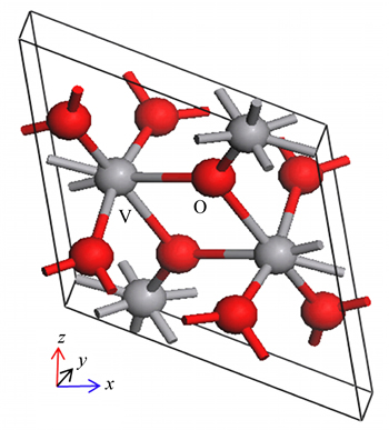
Fig. 1 Cell model of VO2

Fig. 2 Model of Au�CVO2
3 Results and discussion
3.1 Energy band structure and density of states
Figure 3 show the band structures of VO2 (Fig. 3(a)) and Au�CVO2 (Fig. 3(b)). Band gaps of VO2 and Au�CVO2 are found to be 0.115 eV and 0.013 eV, respectively, which are smaller than the theoretical value (0.7 eV) [24]. Smaller band gap values are caused by DFT in GGA functional, which is insufficient to process inter-electron exchange interaction and does not affect the analysis of energy gap results [25]. However, the band gap of VO2 after doping with Au becomes smaller. TIAN et al [26] reported that the band gap of VO2 after W doping decreased from 1.103 eV to 0.643 eV. REN et al [20] reported that the band gap of VO2 after F doping also decreased. The smaller band gap suggests that the doped VO2 has a higher metallicity.

Fig. 3 Band structures of supercell VO2 (a) and Au�CVO2 (b)
The character of energy bands can be evaluated by the density of states. Figure 4 shows the total densities of states of VO2 and Au�CVO2. Figure 5 presents partial densities of states of V atom for VO2 and Au atom for Au�CVO2. The curves of total density of states for VO2 and Au�CVO2 are very similar. The partial densities of state of V atom are mainly made up of four groups. The first group between �C67 eV and -65 eV is from V 4s orbital. The second group between �C40 eV to �C37 eV is from V 4p orbital. The third group between �C7 eV to 0 eV is mainly made up of V 3d orbital. The conduction band is made up of V 3d orbital. The partial densities of state of Au are made up of two groups. The first group between �C0.2 eV and �C0.7eV is mainly composed of Au 5d orbital with few Au 6s orbital. The conduction band is made up of Au 5d orbital.
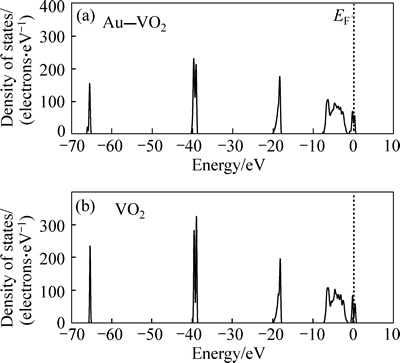
Fig. 4 Total densities of states for VO2 and Au�CVO2
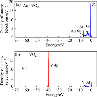
Fig. 5 Density of states of supercell Au�CVO2 and VO2
Figure 6 shows DOS results of interactions between V atom and O atom for VO2, and between Au atom and O atom for Au�CVO2. It is clear that near Fermi level electrons of V��O bond are mainly from O 2p orbital and V 3d orbital; those of Au�CO bond are mainly from O 2p orbital and Au 5d orbital. DOS of Au 5d for Au��O is larger than that of V 3d for V��O bond, showing that Au is more active than V. In addition, the overlap of O 2p and Au 5d orbital is larger than that of O 2p and V 3d orbital. These results show that the interaction between O and Au is stronger than that between O and V.

Fig. 6 DOS results of O atom and V atom for VO2, O atom and Au atom for Au�CVO2
3.2 Mulliken population analysis
Table 1 shows Mulliken bond population values of O��V bond (VO2) and Au��O bond (Au-VO2). It is very clear that the population values of Au��O bond is much smaller than that of V��O bond, which shows that covalent bond between Au and O is weaker than that between O and V. According to Fig. 6, the interaction between O and Au is stronger than that between O and V, indicating that O��Au contains the stronger ionic bond.
Table 1 Mulliken bond population of VO2 and Au�CVO2

3.3 Optcial properties
Figure 7 shows the dielectric functions of VO2 and Au-VO2. The formula of dielectric function is shown as follows:
 (2)
(2)
where ��1(��)=Re��(��); ��2(��)=Im��(��); Re��(��) and Im��(��) are real and imaginary parts of dielectric function, respectively; �� is frequency. According to Fig. 7, the dielectric function of Au-VO2 is very different from VO2. The dielectric peak of Au-VO2 shifts towards the low energy compared toVO2, and the peak intensity of the imaginary part increases; while that of the real part decreases.
Figure 8 shows the conductivities of VO2 and Au�CVO2. It is very obvious that the conductivity of Au�CVO2 is larger than that of VO2, especially those around 1000 nm (imaginary part). The conductivity of polarization current ��p and the dielectric function ��(��) are related through Eq. (3):
 (3)
(3)
According to Eq. (3), the conductivity is proportional to the imaginary part of dielectric function [27], which is in good agreement with the results of dielectric function (Fig. 7) and also with those of band structures in which band gap of Au�CVO2 is smaller (Fig. 3). The conductivity of Au�CVO2 increases with a decrease in band gap. When light is irradiated to a material, the photon energy larger than the band gap can excite electron-hole pair and cause an increase of carrier concentration, resulting in increasing conductivity.
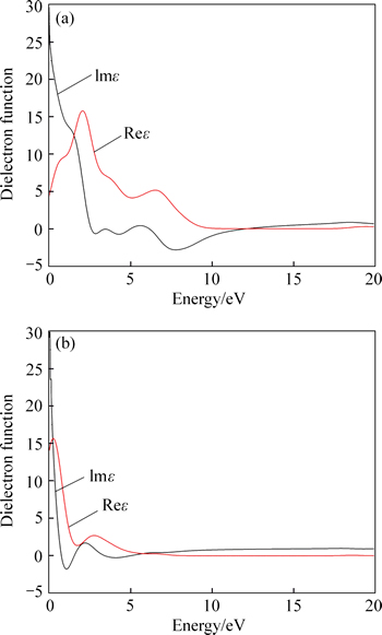
Fig. 7 Dielectric functions of VO2 (a) and Au�CVO2(b)
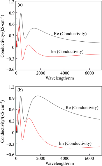
Fig. 8 Conductivities of VO2 (a) and Au�CVO2 (b)
Figure 9 shows the absorption spectra of VO2 and Au�CVO2. The intensity and corresponding wavelength of absorption peak for Au�CVO2 are larger than those of VO2. The larger wavelength of absorption peak for Au�CVO2 means a red-shift relative to VO2. Therefore, the band gap of Au�CVO2 is smaller than that of VO2, which is in good agreement with the results of band structure (Fig. 3). On the other hand, optical absorption coefficient is proportional to the imaginary part of dielectric function [27, 28], which is also in well agreement with our results. In this study, the peak intensity of the imaginary part of dielectric function for Au�CVO2 was found larger, resulting in the increase of intensities of the optical absorption.
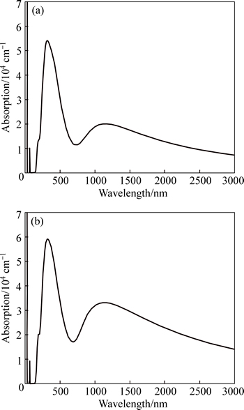
Fig. 9 Optical absorption of VO2 (a) and Au�CVO2 (b)
4 Conclusions
The electronic structure and optical properties of VO2 and Au�CVO2 were studied using density functional theory. The electronic structures and optical properties of VO2 and Au�CVO2 are different. The interaction between Au and O is stronger than that between V and O. There exists not only the covalent bonding but also ionic bonding in Au��O bond. The band gaps of VO2 and Au�CVO2 are 0.115 eV and 0.013 eV, respectively. In other words, when Au is doped in the VO2, the band gap of VO2 becomes small, while the dielectric constant, conductivity, and intensity of optical absorption get large.
References
[1] WU Yan-fei, FAN Le-le, CHEN Shuang-ming, CHEN Shi, CHEN Fei-hu, ZOU Chong-wen, WU Zi-yu. A novel route to realizecontrollable phases in an aluminum (Al3+)-doped VO2 system and the metal�Cinsulatortransition modulation [J]. Materials Letters, 2014, 127: 44�C47.
[2] JOUSHAGHANI A, JEONG J, PARADIS S, ALAIN D, AITCHISON J S, POON J K S. Voltage-controlled switching and thermal effects in VO2 nano-gap junctions [J]. Applied Physics Letters, 2014, 104: 221904.
[3] LEAHU G L, VOTI R L, LARCIPRETE M C, BELARDINI A, MURA F, FRATODDI I, SIBILIA C, BERTOLOTTI M. Semiconductor-metal phase transition of vanadium dioxide nanostructures on silicon substrate [J]. AIP Conference Proceedings, 2014, 1603: 62�C70.
[4] YAMASAKI S, KANKI T, MANCA N, PELLEGRINO L, MARR D, TANAKA H. Metal�Cinsulator transition in free-standing VO2/TiO2 microstructures through low-power Joule heating [J]. Applied Physics Express, 2014, 7: 023201.
[5] FILINCHUK Y, TUMANOV N A, BAN V, JI Heng, WEI Jiang, SWIFT M W, NEVIDOMSKYY A H, NATELSON D. In situ diffraction study of catalytic hydrogenation of VO(2): Stable phases and origins of metallicity [J]. Journal of the American Chemical Society, 2014, 136: 8100�C8109.
[6] ZHENG Jian-yun, BAO Shan-hu, JIN Ping. TiO2(R)/VO2(M)/ TiO2(A) multilayer film as smart window: Combination of energy-saving, antifogging and self-cleaning functions [J]. Nano Energy, 2015, 11: 136�C145.
[7] KARAOGLAN-BEBEK G, HOQUE M N F, HOLTZ M, FAN Z, BERNUSSI A A. Continuous tuning of W-doped VO2 optical properties for terahertz analog applications [J]. Applied Physics Letters, 2014, 105: 201902.
[8] JOUSHAGHANI A, JEONG J, PARADIS S, ALAIN D, AITCHISON J S, POON J K S. Electronic and thermal effects in the insulator-metal phase transition in VO2 nano-gap junctions [J]. Applied Physics Letters, 2014, 105: 231904.
[9] JONES A C, BERWEGER S, WEI Jiang, COBDEN D, RASCHKE M B. Nano-optical investigations of the metal-insulator phase behavior of individual VO(2) microcrystals [J]. Nano Letters, 2010, 10: 1574�C1581.
[10] K R
R M U, YAGLIOGLU G H,
  B, OKSUZOGLU M R, YILDIRIM M,
  M A, PEKDEMIR S, ELMALI A. Excited state dynamics of nanocrystalline VO2 with white light continuum time resolved spectroscopy [J]. Optics Communications, 2014, 333: 109�C114.
[11] LI Ya-mei, JI Shi-dong, GAO Yan-feng, LUO Hong-jie, KANEHIRA M. Core-shell VO2@TiO2 nanorods that combine thermochromic and photocatalytic properties for application as energy-saving smart coatings [J]. Scientific Reports, 2013, 3: 1370.
[12] ZHANG Shu-yan, KATS M A, CUI Yan-jie, ZHOU You, YAO Yu, RAMANATHAN S, CAPASSO F. Current-modulated optical properties of vanadium dioxide thin films in the phase transition region [J]. Applied Physics Letters, 2014, 105: 211104.
[13] LONG Lin-shuang, YE Hong, GAO Yan-feng, ZOU Ru-qiang. Performance demonstration and evaluation of the synergetic application of vanadium dioxide glazing and phase change material in passive buildings [J]. Applied Energy, 2014, 136: 89�C97.
[14] LI Shu-yi, NIKLASSON G A, GRANQVIST C G. Thermochromic fenestration with VO2-based materials: Three challenges and how they can be met [J]. Thin Solid Films, 2012, 520: 3823�C3828.
[15] LV Wei-zhong, HUANG De-zhen, CHEN Yan-mei, QIU Qi, LUO Zhong-kuan. Synthesis and characterization of Mo�CW co-doped VO2(R) nano-powders by the microwave-assisted hydrothermal method [J]. Ceramics International, 2014, 40: 12661�C12668.
[16] FAN Le-le, CHEN Shi, LUO Zhen-lin, LIU Qin-hua, WU Yan-fang, SONG Li, JI D X, WANG Peng, CHU Wang-sheng, GAO Chen, ZOU Chong-wen, WU Zi-yu. Strain dynamics of ultrathin VO2 film grown on TiO2 (001) and the associated phase transition modulation [J]. Nano Letters, 2014, 14: 4036�C4043.
[17]  A, CABRERA R, COY H, MERCED E,
  N,
N,  F E. Phase transition behavior in microcantilevers coated with M1-phase VO2 and M2-phase VO2:Cr thin films [J]. Journal of Applied Physics, 2012, 111: 104502.
[18] HENDAOUI A,  MOND N, DORVAL S, CHAKER M, HADDAD E. VO2-based smart coatings with improved emittance-switching properties for an energy-efficient near room-temperature thermal control of spacecrafts [J]. Solar Energy Materials and Solar Cells, 2013, 117: 494�C498.
[19] LI Shu-yi, MLYUKA N R, PRIMERZHOFER D, HALL N A, POSSNERT G, NIKLASSON G A, GRANQVIST C G. Bandgap widening in thermochromic Mg-doped VO2 thin films: Quantitative data based on optical absorption [J]. Applied Physics Letters, 2013, 103: 161907.
[20] REN Qing-hua, WAN Jin-yu, GAO Yan-feng. Theoretical study of electronic properties of X-doped (X=F, Cl, Br, I) VO2 nanoparticles for thermochromic energy-saving foils [J]. Journal of Physical Chemistry A, 2014, 118: 11114�C11118.
[21] HUANG Zhang-li, CHEN Chang-hong, LV Chao-hong, CHEN Si-hai. Tungsten-doped vanadium dioxide thin films on borosilicate glass for smart window application [J]. Journal of Alloys and Compounds, 2013, 564: 158�C161.
[22] FAN Shao-juan, FAN Le-le, LI Qiang, LIU Jian-dang, YE Bang-jiao. The identification of defect structures for oxygen pressure dependent VO2 crystal films [J]. Applied Surface Science, 2014, 321: 464�C468.
[23] KIM G H, KWAK Y R, LEE I, RATHI S, BAIK J M, YI K S. Conductance control in VO2 nanowires by surface doping with gold nanoparticles [J]. ACS Applied Materials & Interfaces, 2014, 6: 14812�C14818.
[24] GOODEOUGH J B. The two components of the crystallographic transition in VO2 [J]. Journal of Solid State Chemistry, 1971, 3: 490�C500.
[25] SONG Ting-ting, HE Jie, MENG Qi-kai, SUN Peng. Calculation of electronic structure and optical properties of VO2 [J]. The Journal of Light Scattering, 2008, 20(2): 194�C199. (in Chinse)
[26] TIAN Xue-song, WANG Qi,SUN Jian-feng, FAN Zhi-gang. The calculation of doped vanadium dioxide thin films [C]// International Conference on Optoelectronics & Microelectronics. 2013: 242�C244.
[27] HUANG Kun, HAN Ru-qi. Solid state physics [M]. Beijing: Higher Education Press, 1988. (in Chinese)
[28] FAN Ji-ping, LIU Hui-min, TIAN Qiang. The imaginary part of dielectric function and the absorption coefficient [J]. College Physics, 2009, 28(3): 24-25. (in Chinese)
(Edited by YANG Hua)
Cite this article as: HUANG De-wei, ZHAO Cui-hua, CHEN Jian-hua, LI Yu-qiong, LI Wei-zhou. First-principles study of electronic structure and optical properties of Au-doped VO2 [J]. Journal of Central South University, 2017, 24(2): 270-275. DOI: 10.1007/s11171-017-3427-2.
Foundation item: Project(2014GXNSFAA118342) supported by Guangxi Natural Science Foundation, China; Project supported by Open Foundation of Guangxi Key Laboratory for Advanced Materials and Manufacturing Technology, China; Project supported by High-level Innovation Team and Outstanding Scholar Program in Guangxi Colleges (the second batch), China
Received date: 2015-09-21; Accepted date: 2016-03-22
Corresponding author: ZHAO Cui-hua, PhD; E-mail: xiaocui2000110@163.com