Trans. Nonferrous Met. Soc. China 25(2015) 4040-4045
Effect of sintering temperature on microstructure and varistor properties of Zn-V-O-based ceramics incorporated with Mn-Nb-Tb
C. W. NAHM
Semiconductor Ceramics Laboratory, Department of Electrical Engineering, Dongeui University, Busan 47340, Korea
Received 15 April 2015; accepted 13 October 2015
Abstract: The effect of sintering temperature on microstructure and varistor properties of Zn-V-O-based ceramics incorporated with Mn-Nb-Tb was investigated. The results showed that the increase of sintering temperature in the range from 875 to 950 ��C decreased the densities of sintered pellets in the range of 5.55 to 5.45 g/cm3 and increased the average grain size in the range of 4.1 to 8.8 mm. The breakdown field decreased noticeably from 7443 to 1064 V/cm with increasing sintering temperature from 875 to 950 ��C. The varistor ceramics sintered at 900 ��C exhibited nonlinear properties, with 49.4 in the nonlinear coefficient and 0.21 mA/cm2 in the leakage current density. The dielectric constant increased greatly from 440.1 to 2197.2 with increasing sintering temperature from 875 to 950 ��C; however, the dissipation factor exhibited a fluctuation between 0.237 and 0.5. These ceramic compositions and sintering conditions can be applied to the development of advanced multiplayer varistors with silver as an inner electrode.
Key words: Zn-V-O-based ceramics; Mn-Nb-Tb; sintering; varistor properties; dielectric characteristics; varistor
1 Introduction
Zinc oxide is an attractive and smart material, which yields diverse applications such as optical devices, sensor, FET devices, SAW devices, and varistors with a processing method. Among them, we are only interested in varistor effect using zinc oxide. In general, zinc oxide ceramics sintered yield a distinctive microstructure with many grains and grain boundaries. Unit microstructure composed of grain-grain and boundary-grain is distributed into entire bulk with 3-dimensional series and parallel connection.
Pure zinc oxide exhibits a linear voltage (V)-current (I) relation. This is only matter obeying Ohm��s law. If unit microstructure has electronic states inducing potential barrier at the grain boundaries, zinc oxide ceramics will obviously exhibit non-ohmic properties. However, this does not occur for pure zinc oxide under any sintering conditions.
Zinc oxide varistor ceramics are electronic parts made by sintering zinc oxide incorporated with minor oxides composed of main oxide and subordinate oxides [1-4]. A semiconductor junction formed at unit microstructure exhibits non-ohmic properties according to sintering process and additives as variables. They exhibit V-I characteristics similar to a back-to-back Zener diode, with high resistance below breakdown voltage and low resistance above breakdown voltage [2-4]. Owing to simple and distinctive properties, they are extensively utilized to protect the circuit devices from considerably high voltage when compared with normal voltage. Today, all electrical and electronic systems have varistor��s help.
Commercial multilayered chip varistors are strongly based on bismuth [5-9] and praseodymium inducing the varistor effect (nonlinearity) [1,10]. Zinc oxide ceramics incorporated with bismuth and praseodymium should be sintered at high temperatures above 1200 ��C [11,12], and consequently have no choice but to use a refractory such as palladium and platinum as an inner-electrode. But, zinc oxide ceramics incorporated with vanadium inducing the varistor effect have a surprising advantage in terms of inner-electrode silver, when compared with palladium and platinum [13,14]. The studies on Zn-V-O-based ceramics were investigated in many points [15-25]. Nevertheless, it is difficult to use this varisor commercially because of a large number of unsolved problems. Therefore, it is interesting to investigate how the sintering process has an effect on varistor properties for specific composition. In this work, the effects of sintering on microstructure, electrical properties and dielectric characteristics of Zn-V-O- based ceramics incorporated with Mn-Nb-Tb were investigated at temperatures as low as 875-950 ��C.
2 Experimental
High purity (>99.9%, reagent grade) raw materials (in mole fraction) composed of 97.35% ZnO (Aldrich Chemical Co., USA), 0.5% V2O5 (Kojundo Chemical Lab., Japan), 2.0% MnO2 (Kojundo Chemical Lab., Japan), 0.1% Nb2O5 (Kojundo Chemical Lab., Japan), 0.05% Tb4O7 (Kojundo Chemical Lab., Japan) were prepared. Raw materials were mixed by ball milling with zirconia balls and acetone in a polypropylene bottle for 24 h. The blended slurry was dried at 120 ��C for 12 h. The dried slurry was blended with acetone and polyvinyl butyral binder (0.8%, mass fraction based on powder mass) in a beaker using a magnetic stirring bar. After drying, the blend was granulated by sieving through a 0.15 ��m screen to produce starting powder. The sieved powder was pressed into disk-shaped pellets of 10 mm in diameter and 1.5 mm in thickness at a pressure of 100 MPa. The pellets were set on MgO plate into alumina sagger, sintered at different temperatures (875, 900, 925, and 950��C) in air for 3 h, and furnace-cooled to room temperature. The final pellets were roughly 8 mm in diameter and 1.0 mm in thickness. Conductive silver paste was coated by screen-printing techniques on both faces of the pellets and the electrodes were formed by heating it at 550 ��C for 10 min. The electrodes were 5 mm in diameter. Finally, after soldering the lead wire to both electrodes, the samples were packaged by dipping them into a thermoplastic resin powder.
Either side of the samples was lapped and ground with SiC paper, and then polished with 0.3 ��m-Al2O3 powder. The polished samples were chemically etched in HClO4�CH2O solution (1:1000, volume ratio) at 25 ��C for 25 s. The surface microstructure was examined by a field emission scanning electron microscope (FESEM, Quanta 200, FEI, Brno, Czech). The average grain size (d) was determined through the lineal intercept method using the expression: d=1.56L/(MN), where L is the random line length on the micrograph, M is the magnification of the micrograph, and N is the number of the grain boundaries intercepted by the lines [26]. The crystalline phases were identified by X-ray diffractometer (XRD, X��pert-PRO MPD, Panalytical, Almelo, Netherlands) with Cu K�� radiation. The density (r) of sintered pellet was measured using a density determination kit (238490) attached to balance (AG 245, Mettler Toledo International Inc., Greifensee, Switzerland).
The electric field (E)-current density (J) characteristics were measured using a high voltage source-measure unit (Keithley 237, Keithley Instruments Inc., Cleveland, OH, USA). The breakdown field (E1 mA) was measured at a current density of 1.0 mA/cm2 and the leakage current density (JL) was measured at 0.80 E1 mA. The nonlinear coefficient (��) was determined through the expression: ��=(lg J2-lg J1)/(lg E2-lg E1), where E1 and E2 are the electric fields corresponding to J1=1.0 mA/cm2 and J2=10 mA/cm2, respectively. The dielectric behavior in accordance with frequency for the apparent dielectric constant (��'APP) and dissipation factor (tan ��) of the samples was measured in the range of 100 Hz-2 MHz using a RLC meter (QuadTech 7600, Marlborough, MA, USA).
3 Results and discussion
Figure 1 shows the SEM images of the samples at various sintering temperatures. Outwardly, it cannot find a noticeable difference, when compared with the surface morphologies of other ZnO-V2O5-based varistor ceramics [18,19]. However, it can be seen that the grain size noticeably changed despite small changes in the sintering temperature, in particular, at above 900 ��C. The pore was found to increase with increasing sintering temperature. The detailed microstructure parameters are summarized in Table 1.
The tendency of change in the average grain size (d) and the density (r) of the sintered pellets as a function of sintering temperature is indicated graphically in Fig. 2. d increased remarkably from 4.1 to 8.8 ��m despite the variation of small sintering temperature. r decreased from 5.55 to 5.45 g/cm3 to a small extent corresponding to 96.0%-94.3% of the theoretical density (��TD) (for pure ZnO, ��TD=5.78 g/cm3) with increasing sintering temperature from 875 to 950 ��C. It is worth noting that the ceramics with this composition can be sintered at temperatures as low as 875 ��C. This is assumed to be result of the volatility of the V-species for V2O5 with low melting point as low as 690 ��C.
The XRD patterns of the samples at different sintering temperatures are shown in Fig. 3. Many minor phases such as Zn3(VO4)2, ZnV2O4, TbVO4 and VO2 were detected as secondary phases. Among minor phases, VO2 at 2q=28.0650�� almost disappeared when the sintering temperature exceeded 900 ��C. This is assumed to be result of the volatility of liquid phase when the sintering temperature exceeded 900 ��C. The disappearance of VO2 may affect nonlinear properties. In contrast, no TbVO4 was affected by sintering temperature.

Fig. 1 SEM images of samples at various sintering temperatures
Table 1 Average grain size (d), sintered density (r), breakdown field (E1 mA), breakdown voltage per grain boundaries (Vgb), nonlinear coefficient (a), leakage current density (JL), dielectric constant (e��APP) and dissipation factor (tan d) of samples with various sintering temperatures
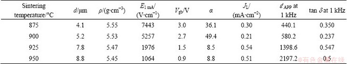
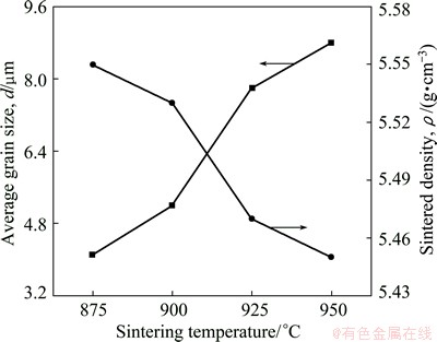
Fig. 2 Average grain size and sintered density of samples as function of sintering temperature
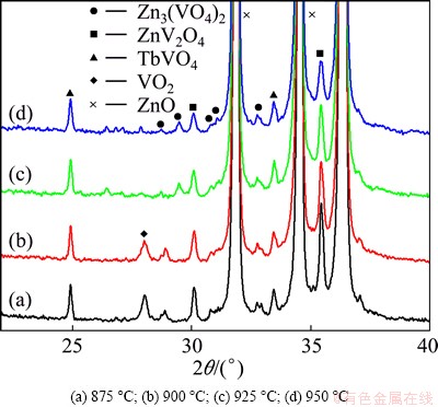
Fig. 3 XRD patterns of samples at various sintering temperatures

Fig. 4 E-J characteristics of samples at various sintering temperatures
Figure 4 shows the electric field-current density (E-J) characteristics of the samples at various sintering temperatures. The varistor properties are featured by the non-linearity, which is not obeyed by Ohm��s law in the E-J relation. The characteristic curves are composed of two states: one is non-conduction state due to extremely high resistance before breakdown field, the other is conduction state due to extremely low resistance after breakdown field. However, the shape of edge between linear region and non-linear region shows an obvious difference with sintering temperature. The detailed E-J characteristic parameters are summarized in Table 1.
The breakdown field (E1mA) showed tendency of abrupt change from 7443 to 1064 V/cm with increasing sintering temperature from 875 to 950 ��C despite small sintering changes. E1mA is firstly controlled by the average grain size (d), and secondly depends on the breakdown voltage per grain boundary (Vgb). The breakdown voltage (VB) is indicated through the expression: VB=(D/d)Vgb=nVgb. As a result, E1mA is written as follows: E1 mA=Vgb/d, where D is the thickness of sample, and n is the number of grain boundaries [2]. Therefore, VB is proportional to n and Vgb. Obviously, the breakdown voltage could be controlled by the sample thickness for the fixed grain size, and by the grain size for the fixed sample thickness. As a result, the decrease of E1mA with increasing sintering temperature is attributed to the increase of the average ZnO grain size and the decrease of Vgb.
The tendency of change in the nonlinear coefficient (��) as a function of sintering temperature is indicated graphically in Fig. 5. �� increased from 36.1 to 49.4 until the sintering temperature reached 900 ��C. When the sintering temperature reached 900 ��C, �� decreased to almost 8.5. However, �� showed the fluctuation in the change tendency with increasing sintering temperature. In light of the change tendency in ��, the sintering temperature in this system has a noticeable effect on non-linear properties although small sintering changes. It is worth noting that the sample sintered at a temperature as low as 875 ��C exhibited a high �� value, reaching ��=36.1. This suggests a potential possibility although low temperature sintering. The behavior of �� in accordance with sintering temperature is directly related to the potential barrier height, which strongly depends on the electronic trap states, such as the zinc vacancies (VZn,) interstitial zinc (Zni,) ionized donor-like zinc (DZn,) and oxygen (Oi) at the grain boundaries [27]. Furthermore, these defects will vary the density of interface states at the grain boundaries. Based on XRD analysis, it is assumed that the disappearance of ZnV2O4 and VO2, when the sintering temperature exceeds 925 ��C, will change the density of interface states, in light of the decrease of nonlinear coefficient.
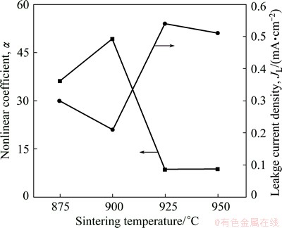
Fig. 5 Nonlinear coefficient and leakage current density as function of sintering temperature
The change tendency in the leakage current density (JL) as a function of sintering temperature is also indicated graphically in Fig. 5. JL decreased from 0.3 to 0.21 mA/cm2 when the sintering temperature increased from 875 to 900 ��C, and then increased to 0.54 mA/cm2 when the sintering temperature was further increased to 925 ��C. However, when the sintering temperature exceeded 925 ��C, it decreased again. JL exhibited a fluctuation in the range of 0.21 to 0.54 mA/cm2 with increasing sintering temperature from 875 to 950 ��C. This is opposite to the behavior of ��. On the whole, it is concluded that the increase of sintering temperature increased JL.
Figure 6 shows the apparent dielectric constant (��'APP) and dissipation factor (tan ��) of the samples with change of sintering temperature. The change tendency in the ��'APP for all the samples with sintering temperature showed typically dielectric dispersion phenomena, which decreases with the increase of frequency. The decrease of ��'APP with increasing frequency is assumed to be a result of the decrease of the number of electric dipole, which can follow to gradually increasing frequency. The variation rate of the dielectric dispersion was remarkably large at frequency lower than 1 kHz when the sintering temperature exceeded 900 ��C. Furthermore, the dielectric dispersion was obvious with increasing sintering temperature. ��'APP increased with increasing sintering temperature in the range of overall frequency. On the other hand, tan �� decreased abruptly until the vicinity of roughly 10 kHz with increasing frequency and exhibited a dielectric absorption peak in the vicinity of 200-300 kHz, and thereafter again decreased. The detailed dielectric parameters are summarized in Table 1.
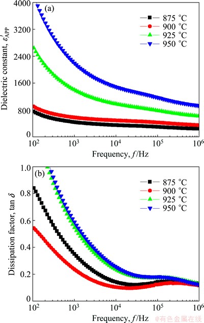
Fig. 6 Dielectric characteristics of samples at various sintering temperatures
The change tendency in ��'APP at 1 kHz as a function of sintering temperature is indicated graphically in Fig. 7. ��'APP increased from 440.1 to 2197.2 although the small variation in the sintering temperature. This is directly related to the average grain size and depletion layer width, as can be seen through the expression, ��'APP= ��g(d/t), where ��g is the dielectric constant of ZnO (8.5), and t is the depletion layer width of the both sides at the grain boundaries. The increase of sintering temperature increases the average grain size (d) and decreases the effective depletion layer width (t). Therefore, the dielectric constant increases with increasing sintering temperature. The change tendency in tan �� at 1 kHz as a function of sintering temperature is also indicated graphically in Fig. 7. tan �� exhibited a fluctuation in the range of 0.237 to 0.547 with increasing sintering temperature. It decreased from 0.350 to 0.237 until the sintering temperature increased from 875 ��C to 900 ��C, and then increased to 0.547 when the sintering temperature was further increased to 925 ��C. However, when the sintering temperature exceeded 925 ��C, it decreased again. On the whole, it is concluded that the increase of sintering temperature increased tan ��. tan �� is composed of the joule loss due to heat generation by leakage current, and frictional loss due to heat generation by electric dipole rotation. The change tendency in tan �� is very similar to that of leakage current. Therefore, it is assumed that tan �� is strongly affected by the leakage current.
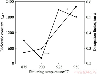
Fig. 7 Dielectric constant (��'APP) and dissipation factor (tan d) as function of sintering temperature at 1 kHz
4 Conclusions
The microstructure, electrical properties and dielectric characteristics of Zn-V-O-based ceramics incorporated with Mn-Nb-Tb were investigated for the samples at various sintering temperatures. Increasing sintering temperature yielded the decrease in the sintered density and the increase in the average grain size, like ceramic behavior of other ZnO-V2O5-based ceramics. The breakdown field decreased noticeably with increasing sintering temperature. The varistor ceramics sintered at 900 ��C exhibited excellent nonlinear properties, with a high nonlinear coefficient (��=49.4). The sintering temperature has a strong effect on nonlinear properties in light of the change tendency in the nonlinear coefficient. The dissipation factor was predominantly generated by the leakage current.
References
[1] MATSUOKA M. Nonohmic properties of zinc oxide ceramics [J]. Japanese Journal of Applied Physics, 1971, 10: 736-746.
[2] LEVINSON L M, PILIPP H R. Zinc oxide varistor��A review [J]. American Ceramic Society Bulletin, 1986, 65: 639-646.
[3] GUPTA T K. Application of zinc oxide varistor [J]. Journal of the American Ceramic Society, 1990, 73: 1817-1840.
[4] CLARKE D R. Varistor ceramics [J]. Journal of the American Ceramic Society, 1999, 82: 485-502.
[5] XU Dong, CHENG Xiao-nong, YAN Xue-hua, XU Hong-xing, SHI Li-yi. Sintering process as relevant parameter for Bi2O3 vaporization from ZnO-Bi2O3-based varistor ceramics [J]. Transactions of Nonferrous Metals Society of China, 2009, 19(6): 1526-1532.
[6] XU Dong, SHI Xiao-feng, CHENG Xiao-nong, YANG Juan, FAN Yue-e, YUAN Hong-ming, SHI Li-yi. Microstructure and electrical properties of Lu2O3-doped ZnO-Bi2O3-based varistor ceramics [J]. Transactions of Nonferrous Metals Society of China, 2010, 20(12): 2303-2308.
[7] XU Dong, TANG Dong-mei, JIAO Lei, YUAN Hong-ming, ZHAO Guo-ping, CHENG Xiao-nong. Effects of high-energy ball milling oxide-doped and varistor ceramic powder on ZnO varistor [J]. Transactions of Nonferrous Metals Society of China, 2012, 22(6): 1423-1431.
[8] XU Dong, TANG Dong-mei, JIAO Lei, YUNA Hong-ming, ZHAO Guo-ping, CHENG Xiao-nong. Comparative characteristics of yttrium oxide and yttrium nitric acid doping on ZnO varistor ceramics [J]. Journal of Central South University, 2012, 19(8): 2094-2100.
[9] XU Dong, WU Jie-ting, JIAO Lei, XU Hong-xing, ZHANG Pei-mei, YU Ren-hong, CHENG Xiao-nong. Highly nonlinear property and threshold voltage of Sc2O3 doped ZnO-Bi2O -based varistor ceramics [J]. Journal of Rare Earths, 2013, 31(2): 158-163.
[10] MUKAE K, TSUDA K, NAGASAWA I. Non-ohmic properties of ZnO-rare earth metal oxide-Co3O4 ceramics [J]. Japanese Journal of Applied Physics, 1977, 16: 1361-1368.
[11] CHEN Guo-hua, LI Ji-le, YANG Yun, YUAN Chang-lie, ZHOU Chang-rong. Microstructure and electrical properties of Dy2O3-doped ZnO-Bi2O3 based varistor ceramics [J]. Materials Research Bulletin, 2014, 50: 141-147.
[12] NAHM C W. The nonlinear properties and stability of ZnO-Pr6O11-CoO-Cr2O3-Er2O3 ceramic varistors [J]. Materials Letters, 2001, 47: 182-187.
[13] TSAI J K, WU T B. Non-ohmic characteristics of ZnO-V2O5 ceramics [J]. Journal Applied Physics, 1994, 76: 4817-4822.
[14] TSAI J K, WU T B. Microstructure and nonohmic properties of binary ZnO-V2O5 ceramics sintered at 900 ��C [J]. Materials Letters, 1996, 26: 199-203.
[15] HNG H H, KNOWLES K M. Knowleges, microstructure and current�Cvoltage characteristics of multicomponent vanadium-doped zinc oxide varistors [J]. Journal of the American Ceramic Society, 2000, 83: 2455-2462.
[16] HNG H H, CHAN P L. Effects of MnO2 doping in V2O5-doped ZnO varistor system [J]. Materials Chemistry Physics, 2002, 75: 61-66.
[17] CHEN Chang-shun. Effect of dopant valence state of Mn-ions on the microstructures and nonlinear properties of microwave sintered ZnO-V2O5 varistors [J]. Journal Materials Science, 2003, 38: 1033-1038.
[18] NAHM C W. DC accelerated aging behavior of Co-Dy-Nb doped Zn-V-M-based varistors with sintering process [J]. Journal Materials Science: Materials in Electronics, 2011, 22: 444-451.
[19] NAHM C W. Sintering effect on pulse aging behavior of Zn-V-Mn-Co-Dy-Nb varistors [J]. Journal of the American Ceramic Society, 2011, 94: 2269-2272.
[20] MING Zhao, YU Shi, SHENG Tian-chang. Grain growth of ZnO-V2O5 based varistor ceramics with different antimony dopants [J]. Journal of the European Ceramic Society, 2011, 31: 2331-2337.
[21] NAHM C W. Effect of sintering process on electrical properties and ageing behavior of ZnO-V2O5-MnO2-Nb2O5 varistor ceramics [J]. Journal Materials Science: Materials in Electronics, 2012, 23: 457-463.
[22] NAHM C W. Major effects on electrical properties of ZnO-V2O5-MnO2-Nb2O5-Er2O3 ceramics with sintering changes [J]. Ceramics International, 2012, 38: 2593-2596.
[23] NAHM C W. Effect of sintering temperature on electrical properties, dielectric characteristics, and aging behavior of ZnO-V2O5-based varistor ceramics modified with Bi2O3 [J]. Journal Materials Science: Materials in Electronics, 2013, 24: 118-124.
[24] NAHM C W. Improvement of aging characteristics of (Mn, Nb, Er)-doped ZnO-V2O5-based varistor ceramics by small sintering changes [J]. Journal Materials Science: Materials in Electronics, 2013, 24: 2228-2233.
[25] MIRZAYI M, HEKMATSHOAR M H. Effect of V2O5 on electrical and microstructural properties of ZnO ceramics [J]. Physica B, 2013, 414: 50-55.
[26] WURST J C, NELSON J A. Lineal intercept technique for measuring grain size in two-phase polycrystalline ceramics [J]. Journal of the American Ceramic Society, 1972, 55: 109-111.
[27] GUPTA T K, CARLSON W G. A grain-boundary defect modelfor instability/stability of a ZnO varistor [J]. Journal of Materials Science, 1985, 20: 3487-3500.
�ս��¶ȶԺ�Mn-Nb-Tb��Zn-V-O���մ�����֯��ѹ�����ܵ�Ӱ��
C. W. NAHM
Semiconductor Ceramics Laboratory, Department of Electrical Engineering, Dongeui University, Busan 47340, Korea
ժ Ҫ���о��ս��¶ȶԺ�Mn-Nb-Tb��Zn-V-O���մ�����֯��ѹ�����ܵ�Ӱ�졣��������������ս��¶���875 ��C���ߵ�950 ��C���ս��մ���Ʒ���ܶ���5.55 g/cm3���͵�5.45 g/cm3����ƽ�������ߴ���4.1 ��m������8.8 ��m��������ǿ��7443 V/cm����������1064 V/cm����900 ��C�ս��ѹ���մ���Ʒ�������Եķ��������ԣ��������ϵ��Ϊ49.4��©�����ܶ�Ϊ0.21 mA/cm2�����ս��¶���875 ��C���ߵ�950 ��Cʱ��Zn-V-O���մ���Ʒ�Ľ�糣����440.1����2197.2������������ı仯��ΧΪ0.237~0.5����ˣ����о���Zn-V-O���մ���ֺ��ս���������������Ϊ�ڵ缫���Ƚ����оƬѹ������Ŀ�����
�ؼ��ʣ�Zn-V-O���մɣ�Mn-Nb-Tb���սѹ�����ܣ�������ԣ�ѹ��������
(Edited by Wei-ping CHEN)
Corresponding author: C. W. NAHM; Tel: +82-51-890-1669; Fax: +82-51-890-1664; E-mail: cwnahm@deu.ac.kr
DOI: 10.1016/S1003-6326(15)64053-5

