Effects of ratio of hydrogen flow on microstructure of hydrogenated microcrystalline silicon films deposited by magnetron sputtering at 100 ��C
��Դ�ڿ������ϴ�ѧѧ��(Ӣ�İ�)2019���10��
�������ߣ������� ������ ������ ��ѩ��
����ҳ�룺2661 - 2667
Key words��hydrogenated microcrystalline silicon films; radio frequency magnetron sputtering; ratio of hydrogen flow; low temperature; microstructure
Abstract: Hydrogenated microcrystalline silicon (��c-Si:H) films were prepared on glass and silicon substrates by radio frequency magnetron sputtering at 100 ��C using a mixture of argon (Ar) and hydrogen (H2) gasses as precursor gas. The effects of the ratio of hydrogen flow (H2/(Ar+H2)%)) on the microstructure were evaluated. Results show that the microstructure, bonding structure, and surface morphology of the ��c-Si:H films can be tailored based on the ratio of hydrogen flow. An amorphous to crystalline phase transition occurred when the ratio of hydrogen flow increased up to 50%. The crystallinity increased and tended to stabilize with the increase in ratio of hydrogen flow from 40% to 70%. The surface roughness of thin films increased, and total hydrogen content decreased as the ratio of hydrogen flow increased. All ��c-Si:H films have a preferred (111) orientation, independent of the ratio of hydrogen flow. And the ��c-Si:H films had a dense structure, which shows their excellent resistance to post-oxidation.
Cite this article as: WANG Lin-qing, ZHOU Yong-tao, WANG Jun-jun, LIU Xue-qin. Effects of ratio of hydrogen flow on microstructure of hydrogenated microcrystalline silicon films deposited by magnetron sputtering at 100 ��C [J]. Journal of Central South University, 2019, 26(10): 2661-2667. DOI: https://doi.org/10.1007/s11771-019-4203-7.

J. Cent. South Univ. (2019) 26: 2661-2667
DOI: https://doi.org/10.1007/s11771-019-4203-7

WANG Lin-qing(������)1, 2, ZHOU Yong-tao(������)3, 4,WANG Jun-jun(������)3, 4, LIU Xue-qin(��ѩ��)3, 4
1. School of Science, Chongqing University of Technology, Chongqing 400054, China;
2. Chongqing Key Laboratory of Green Energy Materials Technology and Systems,Chongqing 400054, China
3. College of Materials Science and Engineering, Chongqing University of Technology,Chongqing 400054, China;
4. Chongqing Collaborative Innovation Center for Brake Tribological Materials, Chongqing 400054, China
 Central South University Press and Springer-Verlag GmbH Germany, part of Springer Nature 2019
Abstract: Hydrogenated microcrystalline silicon (��c-Si:H) films were prepared on glass and silicon substrates by radio frequency magnetron sputtering at 100 ��C using a mixture of argon (Ar) and hydrogen (H2) gasses as precursor gas. The effects of the ratio of hydrogen flow (H2/(Ar+H2)%)) on the microstructure were evaluated. Results show that the microstructure, bonding structure, and surface morphology of the ��c-Si:H films can be tailored based on the ratio of hydrogen flow. An amorphous to crystalline phase transition occurred when the ratio of hydrogen flow increased up to 50%. The crystallinity increased and tended to stabilize with the increase in ratio of hydrogen flow from 40% to 70%. The surface roughness of thin films increased, and total hydrogen content decreased as the ratio of hydrogen flow increased. All ��c-Si:H films have a preferred (111) orientation, independent of the ratio of hydrogen flow. And the ��c-Si:H films had a dense structure, which shows their excellent resistance to post-oxidation.
Key words: hydrogenated microcrystalline silicon films; radio frequency magnetron sputtering; ratio of hydrogen flow; low temperature; microstructure
Cite this article as: WANG Lin-qing, ZHOU Yong-tao, WANG Jun-jun, LIU Xue-qin. Effects of ratio of hydrogen flow on microstructure of hydrogenated microcrystalline silicon films deposited by magnetron sputtering at 100 ��C [J]. Journal of Central South University, 2019, 26(10): 2661-2667. DOI: https://doi.org/10.1007/s11771-019-4203-7.
1 Introduction
Hydrogenated microcrystalline silicon (��c-Si:H) films exhibit excellent properties such as high charge carrier mobility, high electrical conductivity, and good stability. Because of these properties, they have attracted considerable attention for use in transistors, solar cells, and image sensors [1-6]. Many deposition techniques, including hot wire chemical vapor deposition, plasma-enhanced chemical vapor deposition, and magnetron sputtering, have been used to grow ��c-Si:H films at a typical substrate temperature ranging from 200 ��C to 400 ��C [1, 4, 7-11]. Growing ��c-Si:H films at a low substrate temperature (<200 ��C) has a strong practical incentive because low temperature enables the use of substrates, such as glass or plastic, that have low softening or decomposition temperatures [12-15]. Recently, many studies have reported on low temperature growth of ��c-Si:H films [14, 16-18], where many assistant processes, including applying a very high pressure to the plasma [16], adding helium/chlorinated silanes to the plasma [17, 18], and using high flux ion bombardment to magnetron sputtering [14], were adopted to facilitate the nucleation of nanocrystallite. In our previous work, ��c-Si:H films were obtained at a low substrate temperature (100 ��C) via magnetron sputtering without any assistant process [19]. However, the ��c-Si:H films had a complex microstructure, consisting of crystalline and amorphous silicon phases, and grain boundaries. The photoelectric properties can be tailored by the microstructure. Thus, studying microstructure evolution is important [1]. The microstructure of ��c-Si:H films strongly depends on the ratio of hydrogen flow (H2/(Ar+H2)%) in a magnetron sputtering at the substrate temperature ranging from 200 ��C to 400 ��C [11, 20-22]. However, few studies have investigated the microstructure of ��c-Si:H films grown by magnetron sputtering at 100 ��C.
In this study, a series of ��c-Si:H films was deposited on glass and silicon substrates via magnetron sputtering at 100 ��C under different H2/(Ar+H2) flow ratios ranging from 40% to 70%. The effects of the ratio of hydrogen flow on the microstructure were evaluated using spectroscopic ellipsometry, Raman spectroscopy, X-ray diffraction (XRD), Fourier transform infrared spectroscopy (FT-IR), and atomic force microscopy (AFM).
2 Experimental
Glass with dimensions of 3 cm��2 cm��0.1 cm and Si (100) wafer were used as substrates. The substrates were ultrasonically cleaned in acetone and ethanol baths in succession for 20 min, followed by rinsing in deionized water. The ��c-Si:H films were deposited on cleaned substrate by using radio frequency (13.56 MHz) magnetron sputtering technique, which was configured with a Si (99.999%) targets. The surface of substrates was cleaned by sputtering with argon (Ar) for 30 min before deposition process. The base pressure was approximately 3��10-5 Pa, and the pressure in the sputtering process was approximately 1.5 Pa. Deposition was performed at 0.2 Pa with Ar flow rate of 30 sccm and H2 flow rate of 20�C70 sccm, corresponding to the ratio of hydrogen flow in the range of 40%-70%. The radio frequency power was fixed at 200 W.
The thickness of the ��c-Si:H films was determined by a spectroscopic ellipsometer (SE, M-2000DI), and the thickness of all as-deposited films was approximately 200 nm. The crystallinity of the ��c-Si:H films was analyzed by confocal micro-Raman spectroscopy measurements (Renishaw inVia Reflex) operated at an argon laser wavelength of 488 nm. In order to avoid the surface damage, the powder of laser light was kept at 5 mW. The diameter of the laser spot was 2.5 ��m. The crystal structure of the ��c-Si:H films was measured by grazing incidence XRD (Bruker AXS D8) using a Cu K�� radiation source operating at 45 kV and 40 mA. The incident angle was 0.5��. The hydrogen bonding information and hydrogen content were obtained using FT-IR (Thermo Nicolet 6700). For easy detection of IR absorption, the ��c-Si:H films were deposited at (100) silicon wafer. The spectra were recorded in transmittance mode (400-2500 cm-1) with 4 cm-1 resolution. Surface roughness and morphology were observed using CSPM 5500 AFM with a contact mode.
3 Results and discussion
Figure 1 shows the AFM images of the ��c-Si:H films under the different ratios of hydrogen flows ranging from 40% and 70%. The surface of the films deposited at a ratio of hydrogen flow of 40% was relatively smooth. Meanwhile, the surface became rough when the ratio of hydrogen flow increased up to 70%. This result indicated that the structure of films was changed with increasing ratio of hydrogen flow [23, 24]. The RMS roughness of the films is shown in Figure 2. The figure shows that RMS roughness increased with the increase in ratio of hydrogen flow. This is in some way related to the incorporation of crystallites in the amorphous matrix, thereby leading to an increase in the surface roughness [23].
The Raman spectra of ��c-Si:H films as a function of ratio of hydrogen flow were measured (Figure 3(a)). The figure shows that only a single peak was present at 480 cm-1 when the ratio of hydrogen flow was 40%, indicating that the as-deposited Si:H films are in the amorphous phase [25]. When the ratio of hydrogen flow increased up to 50%, a weak peak at approximately 520 cm-1 was observed, which corresponds to the transverse optical (TO) mode of the crystalline silicon. This finding revealed that ��c-Si:H films can be formed under this situation. With a further increase in the ratio of hydrogen flow, the intensities of the peak at approximately 520 cm-1 gradually increased, and the 480 cm-1 peak gradually decreased at the same time. These results indicated that in the as-deposited ��c-Si:H films, an amorphous to crystalline phase transition occurred when the ratio of hydrogen flow increased up to 50%.
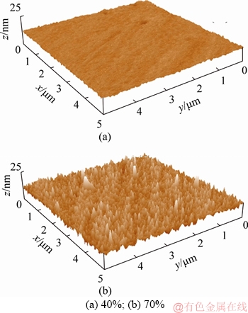
Figure 1 AFM micrographs of ��c-Si:H thin films deposited at various flow rate ratios of hydrogen:
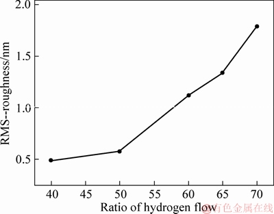
Figure 2 RMS-roughness of ��c-Si:H film as function of ratio of hydrogen flow
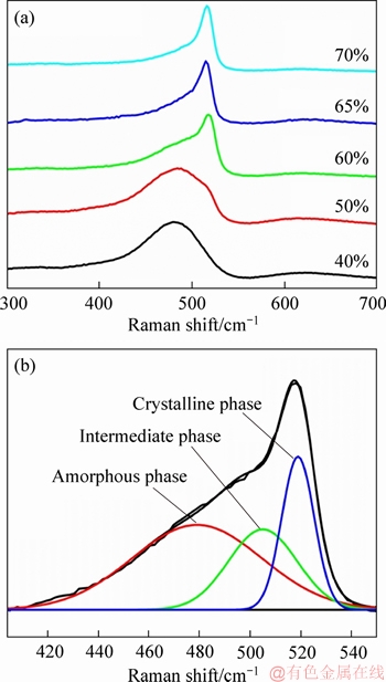
Figure 3 Raman spectra of Si:H thin films deposited under different hydrogen flow ratios (a), Gaussian fitting of ��c-Si:H films prepared with 60% hydrogen flow ratio (b)
The Gaussian fitting of ��c-Si:H films deposited at a ratio of hydrogen flow of 60% is shown in Figure 3(b). The Raman spectrum can be deconvoluted into three peaks located at 520, 510, and 480 cm-1, which belong to the TO mode of the crystalline silicon, defective part of the crystalline phase, and the amorphous silicon phase, respectively [1, 17, 20, 21, 25, 26]. Generally, the approximate fraction of crystalline volume (Xc) of ��c-Si:H films follows the relation [11,20]:
Xc=(I510+I520)/(I480+I510+I520)�� (1)
where the subscript number is wavenumber, and I is the integrated area of the related peak.
Figure 4 shows the Xc of the as-deposited ��c-Si:H films at various ratios of hydrogen flow. Xc increased and tended to stabilize with the increase in ratio of hydrogen flow from 40% to 70%. This phenomenon is caused by various reasons. First, the atomic hydrogen covered on the growing surface can promote ��c-Si:H growth [11, 20, 27]. The increase in the ratio of hydrogen flow indicates an increase in the atomic hydrogen on the growing surface. Second, Ar ion creates hydrogen radicals during the magnetron sputtering deposition of ��c-Si:H. The decrease in Ar ion leads to the decrease in hydrogen radicals [20]. In this work, the Ar flow rate was kept constant. Consequently, hydrogen radicals would be limited by the Ar flow rate. Thus, Xc tended to stabilize when the ratio of hydrogen flow further increased.
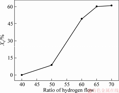
Figure 4 Crystal volume fraction (Xc) of ��c-Si:H thin films deposited under different hydrogen flow ratio
Figure 5 shows the XRD patterns of the ��c-Si:H films as a function of the ratio of hydrogen flow. There is no obvious crystalline diffraction peaks at the ratio of hydrogen flow of 40%, indicating that the as-deposited ��c-Si:H films were amorphous or nearly amorphous. When the ratio of hydrogen flow increased up to 50%, a very weak diffraction peak appeared at approximately 2��=28.4��, corresponding to the Si (111) diffraction peak [1, 18, 28, 29], revealing that the crystal formed under such conditions. With the further increase in ratio of hydrogen flow, the intensities of the peak at approximately 2��=28.4�� gradually increased, and two other small diffraction peaks appeared at approximately 47.3�� and 56.1��, which corresponded to the Si diffraction peaks of (220) and (311) [1, 18, 28, 29], respectively. These results indicated that a transition from the amorphous phase to microcrystalline phase occurred when the ratio of hydrogen flow increased up to 50%. The XRD results were in accordance with the Raman results. Moreover, one could notice that the intensity of the (111) peak became stronger, while the intensities of two other peaks hardly changed with increasing ratio of hydrogen flow. This result indicated that the crystallinity increased with the increase in ratio of hydrogen flow. And all ��c-Si:H films have a preferred (111) orientation, independent of the ratio of hydrogen flow.
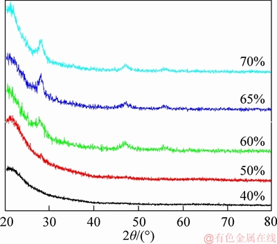
Figure 5 XRD patterns of ��c-Si:H films deposited in various ratios of hydrogen flow
Figure 6 shows the FT-IR spectra of the ��c-Si:H films deposited at various ratios of hydrogen flow. The figure shows that the peak was related to the Si-H wagging/rocking mode located at 640 cm-1 when the ratio of hydrogen flow was <60%. Meanwhile, this peak shifted to ~630 cm-1 for the ��c-Si:H films deposited at the ratio of hydrogen flow of 60%-70%. In addition, the peak related to the stretching absorption band was decomposed into two Gaussian components, ~2010 and ~2090 cm-1. Meanwhile, no absorption band was found at ~2010 cm-1, and the peak at~2090 cm-1 shifted to a higher frequency at the ratio of hydrogen flow of 60%�C70% [14, 22]. The presence of the 630 cm-1 wagging/rocking mode and the high-frequency stretching modes can be attributed either to the presence of Si-H2 and (Si-H2)n complexes at the grain boundaries or to Si-H or Si-H2 bonds located at the (111) and (220) surfaces of the Si crystallites [26, 27]. Furthermore, the peak intensity related to Si-O stretching mode, an indication of materials with low density, was very weak. This indicated that ��c-Si:H films had a dense structure. The dense ��c-Si:H films showed excellent resistance to post-oxidation [14, 22].
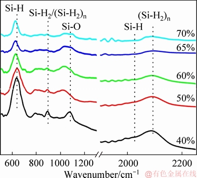
Figure 6 FT-IR absorption spectra of ��c-Si:H films deposited in various ratios of hydrogen flow
Generally, the incorporated hydrogen content in ��c-Si:H films can be estimated from the wagging/rocking mode on the FT-IR absorption spectrum [26, 28, 29]. The total bonded hydrogen concentration (CH) can be calculated using the following relation:
 (2)
(2)
where A640 is the area of the absorption band at 640 cm-1; N is the atomic density of the crystalline silicon (5.0��1022 cm-3); ��(��) is the absorption coefficient [27, 28]. Figure 7 shows the variation of CH for the as-prepared Si:H films. Clearly, CH decreased from 12.0 at% to 4.2 at% when the ratio of hydrogen flow increased from 40% to 70%. This change may be caused by the decrease in the amorphous phase during the growth processes because H mainly bonds with the amorphous matrix [17, 30].

Figure 7 Hydrogen content (CH ) of ��c-Si:H thin films as a function of ratio of hydrogen flow
4 Conclusions
The microstructure of the ��c-Si:H films deposited by RF (13.56 MHz) magnetron sputtering at the low substrate temperature of 100 ��C under different ratios of hydrogen flow was investigated. Amorphous to crystalline phase transition occurs when the ratio of hydrogen flow is approximately 50%. When the ratio of hydrogen flow increases from 40% to 70%, the crystallinity of the ��c-Si:H films increases and tends to stabilize. The surface roughness of thin films increased, and total hydrogen content decreased as the ratio of hydrogen flow increased. These phenomena may be attributed to the increase in atomic hydrogen flux on the growing surface. Moreover, the as-deposited Si:H films had a (111) preferred orientation, independent of the ratio of hydrogen flow. And the ��c-Si:H films had a dense structure, which shows an excellent resistance to post-oxidation.
References
[1] LI T T, XU S Z, HUANG Q, REN H Z, NI J, LI B Z, ZHANG D K, WEI C C, AMANATIDES E, MATARAS D, ZHAO Y, ZHANG X. SiH4 enhanced dissociation via argon plasma assistance for hydrogenated microcrystalline silicon thin-film deposition and application in tandem solar cells [J]. Sol Energ Mat Sol C, 2018, 180: 110�C117. DOI: 10.1016/ j.solmat.2018.02.024.
[2] LIU B, BAI L, LI T, WEI C, LI B, HUANG Q, ZHANG D, WANG G, ZHAO Y, ZHANG X. High efficiency and high open-circuit voltage quadruple-junction silicon thin film solar cells for future electronic applications [J]. Energy Environ Sci, 2017, 10: 1134�C1141. DOI: 10.1039/C7EE00332C.
[3] ZHONG C L, GENG K W, LUO L E, YANG D W. An analytical model to explore open-circuit voltage of a-Si:H/c-Si heterojunction solar cells [J]. Journal of Central South University, 2016, 23: 598�C603. DOI: 10.1007/s11771-016- 3106-0.
[4] SU Y J, DOND C, ZHU M, XU J, FAN P H. Effects of growth temperature on ��c-Si:H films prepared by plasma assistant magnetron sputtering [J]. Rare Metals, 2012, 31(2): 193�C197. DOI: 10.1007/s12598-012-0490-y.
[5] PYTHON M, MADANI O, DOMINE D, MEILLAUD F, VALLAT-SAUVAIN E, BALLIF C. Influence of the substrate geometrical parameters on microcrystalline silicon growth for thin-film solar cells [J]. Sol Energ Mat Sol C, 2009, 93(10): 1714�C1720. DOI: 10.1016/j.solmat. 2009.05.025.
[6] BUGNON G, FELTRIN A, MEILLAUD F, BAILAT J, BALLIF C. Influence of pressure and silane depletion on microcrystalline silicon material quality and solar cell performance [J]. J Appl Phys, 2009, 105(6): 064507. DOI: 10.1063/1.3095488.
[7] ADHIKARI D, JUNDA M M, MARSILLAC S X, COLLINS R W, PODRAZA N J. Nanostructure evolution of magnetron sputtered hydrogenated silicon thin films [J]. J Appl Phys, 2017, 122(7): 075302. DOI: 10.1063/1.4998455.
[8] WANG L Q, WANG W Y, HUANG J H, TAN R Q, SONG W J, CHEN J M. Growth and properties of hydrogenated microcrystalline silicon thin films prepared by magnetron sputtering with different substrate temperatures [J]. Rare Metals, 2015. DOI: 10.1007/s12598-015-0510-9.
[9] DUSHAQ G, NAYFEH A, RASRAS M. Tuning the optical properties of RF-PECVD grown ��c-Si:H thin films using different hydrogen flow rate [J]. Superlattice Microst, 2017, 107: 172�C177. DOI: 10.1016/j.spmi.2017.03.052.
[10] KLEIN S, REPMANN T, BRAMMER T. Microcrystalline silicon films and solar cells deposited by PECVD and HWCVD [J]. Sol Energy, 2004, 77(6): 893�C908. DOI: 10.1016/ j.solener.2004.08.029.
[11] FUKAYA K, TABATA A, SASAKI K. Mechanism of hydrogenated microcrystalline Si film deposition by magnetron sputtering employing a Si target and H2/Ar gas mixture [J]. Jpn J Appl Phys, 2014, 48(3): 035507. DOI: 10.1143/JJAP.48.035507.
[12] MELLOS A, KANDYLA M, PALLES D, KOMPITSAS M. Effects of hydrogen pressure on hydrogenated amorphous silicon thin films prepared by low-temperature reactive pulsed laser deposition [J]. Phys Status Solidi C, 2017, 14(1, 2): 1600088. DOI: 10.1002/pssc.201600088.
[13] ALPUIM P, CHU V, CONDE J P. Amorphous and microcrystalline silicon films grown at low temperatures by radio-frequency and hot-wire chemical vapor deposition [J]. Jpn J Appl Phys, 1999, 86(7): 3812. DOI: 10.1063/1.371292.
[14] GERBI J E, ABELSON J R. Low temperature magnetron sputter deposition of polycrystalline silicon thin films using high flux ion bombardment [J]. Jpn J Appl Phys, 2007, 101(6): 063508. DOI: 10.1063/1.2710301.
[15] WADIBHASME N A, DUSANE R O. Low temperature deposition of device-quality silicon thin films for flexible PV application [C]// 40th IEEE Photovoltaic Specialist Conference. Denvor: IEEE 2014: 3060-3064. DOI: 10.1109/PVSC.2014.6925581.
[16] DAVIS W A, LEWIN G, DAVIS T M E, BRUCE D G. Nanocrystalline Si:H thin films grown at room temperature with plasma-enhanced chemical vapour deposition at a very high pressure [J]. J Phys D Appl Phys, 2012, 45(33): 335104. DOI: 10.1088/0022-3727/45/33/335104.
[17] ZHANG L, GAO J H, XIAO J Q, WEN L S, GONG J, SUN C. Low-temperature (120 ��C) growth of nanocrystalline silicon films prepared by plasma enhanced chemical vapor deposition from SiCl4/H2 gases: Microstructure characterization [J]. Appl Surf Sci, 2012, 258(7): 3221�C3226. DOI: 10.1016/j.apsusc.2011.11.068.
[18] BHATTACHARYA K, DAS D. Effect of deposition temperature on the growth of nanocrystalline silicon network from helium diluted silane plasma [J]. J Phys D Appl Phys, 2008, 41(15): 155420. DOI: 10.1088/0022-3727/ 41/15/155420.
[19] WANG L, WANG W, HUANG J, ZENG Y, TAN R, SONG W, CHEN J. Low temperature magnetron sputtering deposition of hydrogenated microcrystalline silicon thin films without amorphous incubation layers on glass [J]. J Non-Cryst Solids, 2014, 388(3): 86�C90. DOI: 10.1016/ j.jnoncrysol.2014.01.038.
[20] MAKIHARA H, TABATA A, SUZUOKI Y, MIZUTANI T. Effect of the hydrogen partial pressure ratio on the properties of ��c-Si:H films prepared by rf magnetron sputtering [J]. Vacuum, 2000, 59(2): 785�C791. DOI: 10.1016/S0042- 207X(00)00348-1.
[21] GONCALVES C, CHARVET S, ZEINERT A, CLIN M, ZELLAMA K. Nanocrystalline silicon thin films prepared by radiofrequency magnetron sputtering [J]. Thin Solid Films, 2002, 403-404: 91�C96. DOI: 10.1016/s0040-6090(01)01553-x.
[22] FUKAYA K, TABATA A, MIZUTANI T. Dependence on gas pressure of ��c-Si:H prepared by RF magnetron sputtering [J]. Vacuum, 2004, 74(3, 4): 561�C565. DOI: 10.1016/j.vacuum.2004. 01.027.
[23] GOPE J, KUMAR S, SUDHAKAR S, RAUTHAN C M S, SRIVASTAVA P C. Effect of silane flow rate on structural, electrical and optical properties of silicon thin films grown by VHF PECVD technique [J]. Mater Chem Phys, 2013, 141(1): 89�C94. DOI: 10.1016/j.matchemphys.2013.04.028.
[24] GUO L, DING J, YANG J, CHENG G, LING Z. Effects of high hydrogen dilution ratio on surface topography and mechanical properties of hydrogenated nanocrystalline silicon thin films [J]. Thin Solid Films, 2011, 519(18): 6039�C6043. DOI: 10.1016/j.tsf.2011.04.117.
[25] CHENG Q, XU S, OSTRIKOV K K. Structural evolution of nanocrystalline silicon thin films synthesized in high-density, low-temperature reactive plasmas [J]. Nanotechnology, 2009, 20-21: 215606. DOI: 10.1088/0957-4484/20/21/215606.
[26] CHENG Q, XU S, HUANG S, OSTRIKOV K. Effective control of nanostructured phases in rapid, room-temperature synthesis of nanocrystalline Si in high-density plasmas [J]. Cryst Growth Des, 2009, 9(6): 2863�C2867. DOI: 10.1021/ cg900176c.
[27] MATSUDA A. Microcrystalline silicon: Growth and device application [J]. J Non-Cryst Solids, 2004, 338(1): 1�C12. DOI: 10.1016/j.jnoncrysol.2004.02.012.
[28] WEI D Y, XIAO S Q, HUANG S Y, CHAN C S, ZHOU H P, XU L X, GUO Y N, CHAI J W, WANG S J, XU S. Low-temperature deposition of ��c-Si:H thin films by a low-frequency inductively coupled plasma for photovoltaic applications [J]. J Phys D Appl Phys, 2013, 46(21): 215501. DOI: 10.1088/0022-3727/46/21/215501.
[29] XIAO S Q, XU S, WEI D Y, HUANG S Y, ZHOU H P, XU Y. From amorphous to microcrystalline: Phase transition in rapid synthesis of hydrogenated silicon thin film in low frequency inductively coupled plasmas [J]. J Appl Phys, 2010, 108(11): 113520. DOI: 10.1063/1.3514006.
[30] CHENG Q, XU S, OSTRIKOV K. Rapid, low-temperature synthesis of nc-Si in high-density, non-equilibrium plasmas: Enabling nanocrystallinity at very low hydrogen dilution [J]. J Mater Chem, 2009,19(29): 5134�C5140. DOI: 10.1039/b904227j.
(Edited by HE Yun-bin)
���ĵ���
��ϡ�ͱȶԴſؽ������(100 ��C)�����⻯���象Ĥ�ṹ���Ե�Ӱ��
ժҪ���ڵ���(100 ��C)�����²��ôſؽ����ڲ�����(100)�ĵ��ϳ����⻯����(��c-Si:H)��Ĥ���о���ͬ��ϡ�ͱȶ����象Ĥ�ṹ���Ե�Ӱ�졣�����������Ĥ�ӷǾ�����ɵ������൱��ϡ�ͱ����ӵ�Լ50%���⻯���象Ĥ�Ľᾧ������ϡ�ͱȴ�40%���ӵ�70%�����Ӻ������ȶ�����Ĥ�ı���ֲڶ�������ϡ�ͱȵ����Ӷ����ӣ��⺬���ı仯������֮�෴�����Ʊ����⻯���象Ĥ������ (111)����ȡ������ϡ�ͱ��أ��ұ�Ĥ�ṹ���ܡ�
�ؼ��ʣ����象Ĥ����Ƶ�ſؽ��䣻��ϡ�ͱ��������£��ṹ
Foundation item: Projects(51505050, 51805063) supported by the National Natural Science Foundation of China for Young Scholars; Projects(KJ1500942, KJQN201801134) supported by the Scientific and Technological Research Program of Chongqing Education Commission of China; Projects(cstc2017jcyjAX0075, cstc2015jcyjA50033) supported by the Chongqing Research Program of Basic Research and Frontier Technology, China
Received date: 2018-09-02; Accepted date: 2019-02-27
Corresponding author: WANG Jun-jun, PhD, Associate Professor; Tel: +86-2362563175; E-mail: wangjunjun@cqut.edu.cn; ORCID: 0000-0001-5796-8926

