Trans. Nonferrous Met. Soc. China 23(2013) 562-566
Dilute H2SO4 solution for copper seed cleaning in electroplating
Youn-Seoung LEE1, Jae-Sik YOON1, Yang-Rae JO1, Heesoo LEE2, Sa-Kyun RHA3
1. Department of Information Communication Engineering, Hanbat National University, Daejeon 305-719, Korea;
2. School of Materials Science and Engineering, Pusan National University, Busan 609-735, Korea;
3. Department of Materials Science and Engineering, Hanbat National University, Daejeon 305-719, Korea
Received 2 May 2012; accepted 24 September 2012
Abstract: The effects of surface cleaning to eliminate the surface oxides formed on Cu seed layer with dilute H2SO4 solution were investigated. Cu seed layer formed on Ti/Si(100) wafer by sputter deposition was exposed to air to grow native Cu oxide. Dilute H2SO4 solutions and/or TS-40A alkaline soak cleaner were used to remove the native Cu-oxide. After mainly carbon groups (such as C=O) on surface of Cu seed layer were removed by pretreatment of TS-40A alkaline solution, subsequently, dilute H2SO4 acid solution removed Cu-oxides (Cu2O and CuO) as well as a lot of O=C and Cu(OH)2.
Key words: pretreatment; copper-oxide; H2SO4; XPS; sheet resistance
1 Introduction
A copper (Cu) seed layer in electroplating provides a conduction path for the electroplating current. Electroplating is an electro-deposition process for producing a dense, uniform, and adherent coating, usually of metal or alloys, upon a surface by the act of electric current [1-5]. In order to form electroplated Cu film, a Cu seed layer is necessary because it is very difficult to nucleate Cu grains from an aqueous Cu solution on Si or diffusion barrier materials such as Ti, Ta, TiN or TaN [6].
In general, the electroplating current flowing through an oxide layer is decreased with increasing the oxide film thickness because areas covered by surface oxide such as native Cu oxide resist the transfer of surface charge. That is, the current flowing through a Cu seed layer is dependent upon the surface states of Cu seed layer. Therefore, the Cu seed layer should be highly pure. The Cu seed layer requires a low electrical resistivity, low level of impurities, smooth interface, good adhesion to the barrier metal and low thickness concurrent with coherence for ensuring void-free filling [7]. However, Cu oxides form easily on the surface of Cu film due to its high affinity with oxygen and no self-passivation layer forming to prevent the underlying Cu from further oxidation [8]. An oxide layer formation on the surface of Cu seed layer will deteriorate in mechanical and electrical properties of plated film. Therefore, Cu seed layer to be plated may be carried out a variety of pretreatment process such as surface cleaning, surface modification, and rinsing. The purpose of surface pretreatment is to remove contaminants such as native oxide.
Wet chemical cleaning process is one of the widely used cleaning techniques which includes solvent degreasing, alkaline soak cleaning, and acid cleaning. In general, it was known that H2SO4solution is useful for removal of Cu oxide [9]. The chemical reactions of H2SO4 solution with Cu-oxide is as follows: CuO (s)+ H2SO4 (aq)→CuSO4 (aq)+H2O (l) [9].
In this study, the changed surfaces of Cu seed layer were investigated by pretreatment of dilute H2SO4 solutions for removal of native Cu oxide formed on the Cu seed layer.
2 Experimental
Cu seed wafer was exposed to air to grow the native oxide of Cu. In order to remove native Cu-oxide on Cu seed layer, we carried out the alkaline and H2SO4 acid cleaning methods. Cu seed layer (20 nm) on Ti diffusion-adhesion barrier film (20 nm)/p-type Si (100) was deposited by sputter deposition.
In the case of H2SO4 dipping with TS-40A solution pretreatment, firstly, the alkaline cleaning for removal of organic matters of film surface was performed by soaking the wafer in a Metex TS-40A (MacDermid, Inc.) solution for 60 s, and then the wafers were dipped in deionized (DI) water for 20 s with stirring. Zn acid cleaning process, the films pretreated by TS-40A alkaline solution for 60 s were dipped in diluted H2SO4 (95%, Sigma Aldrich Co.) solution (the volume ratio of 1:20 of H2SO4 to DI water) for various cleaning (dipping) time. Also, all wafers were performed DI water rinsing three times for 20 s with stirring and dried in a continuous N2 stream.
According to dipping time in dilute H2SO4 solution, the changed surfaces of Cu seed layer were measured by using surface analysis tools such as scanning electron microscopy (SEM, Hitachi, Japan, Model S-25OOC) and X-ray photoelectron spectroscopy (XPS, PHI VersaProbe XPS Microprobe) at Hanbat National University in Korea. The used X-ray source was the monochromatized Al Kα (1486.6 eV). The binding energy was calibrated to Cu 2p3/2 at 932.6 eV for the Cu films. All XPS data were obtained without Ar+ cleaning.
3 Results and discussion
Figure 1 shows FE-SEM images of the Cu seed layer surface after pretreatments. By the dipping of H2SO4 for 120 s after TS-40A pretreatment, the grain structure showed more clearly than the image by only TS-40A pretreatment (Fig. 1(b)) or bare Cu seed wafer (Fig. 1(a)). This clearer image of grain structure after H2SO4dipping could mean a surface cleaning and/or an elimination of surface contaminants.
In order to investigate the surface chemical states of Cu seed layer by H2SO4dipping, the XPS spectra were obtained. Normalized survey spectra of samples are shown in Fig. 2. As shown in Fig. 2, after TS-40A pretreatment, the intensity of carbon peak decreased abruptly, the intensity of Cu 2p peak increased, but the intensity of O 1s peak decreased very little in comparison with the survey spectrum of bare seed. It can be guessed that the TS-40A as an alkaline soak cleaner removes light dirt and other organic contaminations on the surface of Cu seed layer. From the result, the carbon on Cu seed layer was removed mainly by TS-40A pretreatment. In addition, by H2SO4 treatment after TS-40A pretreatment, the intensity of O 1s peak decreased clearly and the Cu 2p peak intensity increased abruptly. The increase of Cu 2p peak with the decrease of O 1s peak indicates a removal of Cu oxides.
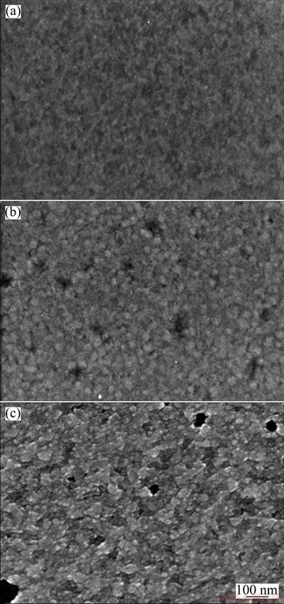
Fig. 1 FE-SEM images of bare Cu seed layer before pretreatment (a), Cu seed layer after pretreatment of only TS-40A for 60 s (b) and by H2SO4 dipping for 120 s after TS-40A pretreatment for 60 s (c)
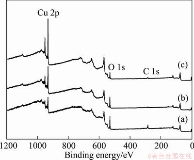
Fig. 2 Normalized XPS survey spectra for bare Cu seed without pretreatment (a), Cu seed wafers by only TS-40A pretreatment for 60 s (b) and by H2SO4 treatment for 120 s after TS-40A for 60 s (c)
In order to estimate the chemical states in Cu site, Cu 2p3/2 narrow spectra of pretreated Cu seed layer are shown in Fig. 3. The main peak at 932.6 eV of Cu 2p3/2 corresponds to metallic Cu or Cu2O and the broad shoulder peaks are formed from CuO (933.6 eV) and Cu(OH)2(~935 eV) [10-12]. In Fig. 3(a), the shoulder peak disappeared by H2SO4 dipping after TS-40A pretreatment. After only TS-40A alkaline cleaning for 60 s, Cu main peak increased a little, a deep occurred at ~934 eV, but the intensity by Cu-OH hardly changed as shown in Fig. 3(b) in more details. From this result, it is found that TS-40A alkaline solution can remove CuO as well as carbon because the deep position at ~934 eV corresponds to CuO state. In addition, the main peak increased abruptly and the shoulder peak disappeared by H2SO4 dipping for 30 s after TS-40A pretreatment. By this result, it is found that H2SO4 solution can remove also Cu-OH group.
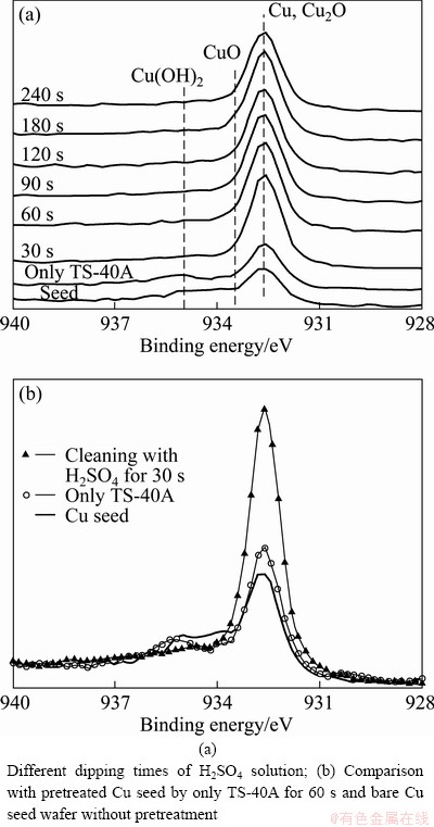
Fig. 3 Cu 2p3/2 XPS narrow spectra of Cu seed layer by H2SO4 solution dipping after TS-40A pretreatment for 60 s
In Fig. 4(a), the intensity and the shape of O 1s peak decreased and changed into double peaks, respectively, after just TS-40A pretreatment. In double peaks, one peak of higher binding energy corresponds to Cu(OH)2 (532.3 eV) and O=C (531.7 eV) and another peak of lower binding energy corresponds to mainly Cu2O (530. 4 eV) with a little CuO (529.6 eV) [10-12]. After only TS-40A pretreatment for 60 s, double peaks showed as the higher binding energy peak decreased, as shown in Fig. 4(b). This result means that TS-40A alkaline solution gets rid of O=C and Cu(OH)2on the surface of Cu seed. However, TS-40A alkaline solution removed carbon and CuO from the results in Figs. 2 and 3. Therefore, it can be concluded that TS-40A alkaline solution can remove mainly O=C rather than Cu―OH group. In addition, by 30 s H2SO4 dipping after 60 s TS-40A pretreatment, the higher binding energy peak decreased more and the lower binding energy peak also decreased a little, as shown in Fig. 4(b). After 60 s H2SO4 dipping (Fig. 4(a)), both of double peaks decreased a little more. From the result, it is found that H2SO4 solution not only removes Cu-oxides (Cu2O and CuO) but also eliminates a lot of O=C and Cu(OH)2 when the solution reacts with the surface of contaminated Cu seed.
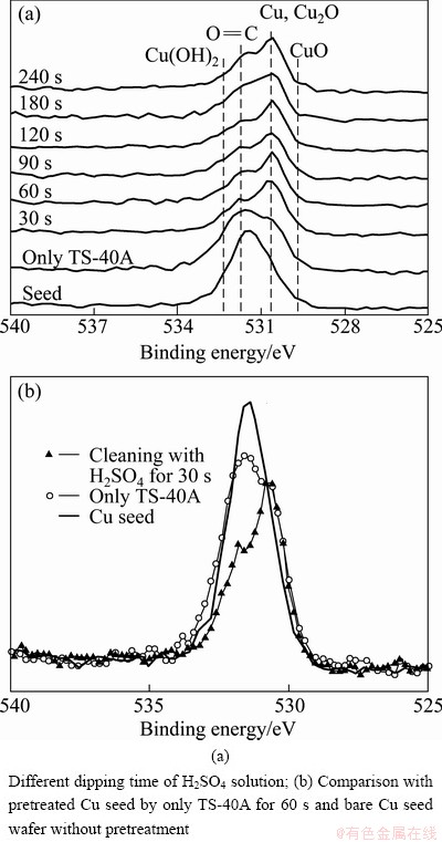
Fig. 4 O 1s XPS narrow spectra of Cu seed layer by H2SO4 solution dipping after TS-40A for 60 s pretreatment
The chemical states in Cu and O sites on surface of Cu seed layer after different dipping time are shown in Figs. 3 and 4. On the other hand, when the time in H2SO4solution was longer than 30 s, both Cu 2p and O 1s peaks hardly changed. This similar surface state may be due to some air contamination by air exposure before XPS measurement because all XPS data were obtained without Ar+ sputtering.
In order to define a removal state of Cu seed layer, XPS depth profiling was carried out. As shown in Fig. 5, the thickness of top Cu seed layer by H2SO4 dipping after TS-40A pretreatment decreased in comparison with Cu seed layer after only TS-40A pretreatment. In addition, oxygen contents by air exposure were always similar on surface and interface. Even if Cu oxide layer is removed by chemical etching, this Cu oxide layer forms always on the surface by air exposure. Considering the 20 nm thickness of bare Cu seed layer in Fig. 5, the etched thickness was ~ 2.7 nm by H2SO4 treatment for 120 s after TS-40A pretreatment.
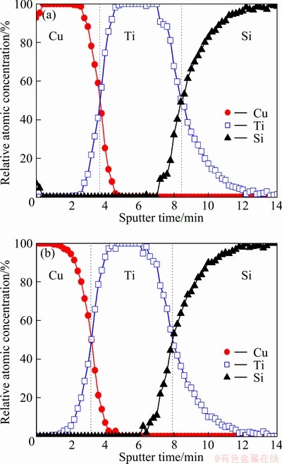
Fig. 5 XPS depth profile of samples pretreated by only TS-40A (60 s) (a) and treated by H2SO4 (120 s) (b) after TS-40A (60 s) pretreatment
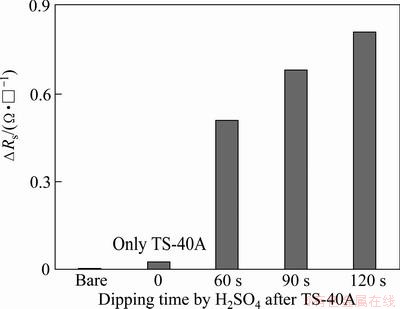
Fig. 6 Difference of sheet resistance △Rs as function of dipping time in H2SO4 solution after TS-40A pretreatment
Figure 6 shows the difference of sheet resistance (ΔRs) using 4-point probe according to H2SO4 dipping time. The ΔRs of samples increased with increasing dipping time compared with Rs values of initial Cu seed layer. Sheet resistance is in inverse proportion to film thickness (t) and proportional to resistivity (ρ): Rs=ρ/t. Therefore, an increase of Rs value in a sample can occur due to an increase of surface resistivity or a decrease of thickness of film. If we assume that the Cu oxides on film surface are eliminated completely, the resistivity of film will decrease. Then, Rs value of film has to decrease. However, Rs of all samples increased although a part of Cu oxide layer was removed by XPS result. This indicates that the increase of Rs is mainly due to the decrease of film thickness. Therefore, we can say that the increase of ΔRs in Fig. 6 is due to the decrease of film thickness. This result agrees well with the result of XPS depth profiling.
4 Conclusions
The surface morphology, surface chemical states, depth profiling, and sheet resistance of Cu seed layer by dilute H2SO4 solution dipping after TS-40A pretreatment were investigated. By pretreatment of TS-40A alkaline solution, at first, mainly carbon groups (such as C=O) on the surface of Cu seed layer were removed. Subsequently, dilute H2SO4 acid solution not only removes Cu-oxides (Cu2O and CuO) but also eliminates a lot of O=C and Cu(OH)2 when the solution reacts with the surface of contaminated Cu seed. The thickness of Cu seed layer decreased from 20 nm to 17.3 nm by H2SO4 treatment for 120 s after TS-40A pretreatment, but there was no decrease of thickness by only TS-40A pretreatment. That is, the etched thickness was ~ 2.7 nm by H2SO4 treatment for 120 s. The ΔRs of the samples increased with increasing the dipping time compared with Rs value of initial Cu seed layer. The increase of ΔRs of the samples depended on the decrease of film thickness. From these results, it is found that dilute H2SO4 solution can remove effectively a native Cu oxide grown by air exposure.
Acknowledgments
This work was supported by the Basic Science Research Program through the National Research Foundation of Korea (NRF) funded by the Ministry of Education, Science and Technology (No. 2012026094).
References
[1] DONNELLY V M, GROSS M E. Copper metalorganic chemical vapor deposition reactions of hexafluoroacetylacetonate Cu(I) vinyltrimethylsilane and bis (hexafluoroacetylacetonate) Cu(II) adsorbed on titanium nitride [J]. Journal of Vacuum Science Technology A, 1993, 11: 66-77.
[2] CHIOU J C, JUANG K C, CHEN M C. Processing windows for selective copper chemical vapor deposition from Cu (hexafluoroacetylacetonate) trimethylvinylsilane [J]. Journal of Electrochemical Society, 1995, 142: 177-182.
[3] MUSIL J, BELL A J, CEPERA M. Deposition of copper films by unbalanced d.c. magnetron sputtering [J]. Czchoslovak Journal of Physics, 1995, 45: 249-261.
[4] KIM S K, KIM J J. Superfilling evolution in Cu electrodeposition- dependence on the aging time of the accelerator [J]. Electrochemcial and Solid-State Letters, 2004, 7: C98-C100.
[5] DOW W P, YEN M Y, LIAO S Z, CHIU Y D, HUANG H C. Filling mechanism in microvia metallization by copper electroplating [J]. Electrochimica Acta, 2008, 53: 8228-8237.
[6] MARTYAK N M, RICOU P. Seed layer corrosion of damascene structures in copper sulfate electrolytes [J]. Materials Science in Semiconductor Processing, 2003, 6: 225-233.
[7] OH J, LEE J, LEE C. Plasma pretreatment of the Cu seed layer surface in Cu electroplating [J]. Materials Chemistry and Physics, 2002, 73: 227-234.
[8] GAO J, HU A, LI M, MAO D. Influence of crystal orientation on copper oxidation failure [J]. Applied Surface Science, 2009, 255: 5943-5947.
[9] GILMAN A F Jr, A. M. Inorganic reactions [M]. Chicago: Eclectic Publishers, 1930: 53.
[10] PELISSIER B, BEAURAIN A, FONTAINE H, DANEL A, JOUBERT O. Investigations on HCl contaminated Cu 200 mm wafers using parallel angle resolved XPS [J]. Microelectronic Engineering, 2009, 86: 1013-1016.
[11] MOULDER J F, STICKLE W F, SOBOL P E, BOMBEN K D. Handbook of X-ray photoelectron spectroscopy [M]. USA: Physical Electronics Inc, 1995.
[12] JUNG S, PARK H, KIM H. Investigation of the bonding states of the SiO2 aerogel film/metal interface [J]. Thin Solid Films, 2004, 447-448: 575-579.
稀硫酸溶液清洗电镀铜晶种
Youn-Seoung LEE1, Jae-Sik YOON1, Yang-Rae JO1, Heesoo LEE2, Sa-Kyun RHA3
1. Department of Information Communication Engineering, Hanbat National University, Daejeon 305-719, Korea;
2. School of Materials Science and Engineering, Pusan National University, Busan 609-735, Korea;
3. Department of Materials Science and Engineering, Hanbat National University, Daejeon 305-719, Korea
摘 要:采用稀硫酸溶液清洗以除去在铜晶种表面形成的氧化物。将通过溅射沉积在Ti/Si(100)薄片上生成的铜晶种暴露在空气中来生长原生铜氧化物。用稀硫酸溶液和TS-40A碱性清洗剂除去原生铜氧化物。先用TS-40A碱性清洗剂预处理以除去铜晶种表面的有机物,再用稀硫酸溶液除去铜氧化物(Cu2O和CuO)以及有机物和Cu(OH)2。
关键词:预处理;铜氧化物;H2SO4;光电子能谱;方块电阻
(Edited by Hua YANG)
Corresponding author: Sa-Kyun RHA; E-mail: skrha@hanbat.ac.kr
DOI: 10.1016/S1003-6326(13)62500-5

