单晶铜纳米加工过程中热效应及缺陷结构的原子尺度模拟
来源期刊:中国有色金属学报(英文版)2012年第11期
论文作者:郭永博 梁迎春
文章页码:2762 - 2770
关键词:单晶铜;原子尺度模拟;热效应;分子动力学模拟;纳米加工;温度分布;缺陷结构;位错;空位
Key words:monocrystalline copper; atomistic simulation; thermal effects; molecular dynamics simulation; nanomachining; temperature distribution; defect structures; dislocations; vacancies
摘 要:基于建立的新型三维仿真模型,采用分子动力学方法模拟单晶铜(100)表面纳米加工过程,研究材料的去除机理和纳米加工过程中系统的温度分布与演化规律。仿真结果表明:系统的温度分布呈同心型,切屑温度最高,并且在金刚石刀具中存在较大的温度梯度。采用中心对称参数法区分工件中材料缺陷结构的形成与扩展。位错和点缺陷是纳米加工过程中工件内部的主要缺陷结构。工件中的残余缺陷结构对于工件材料的物理属性和已加工表面质量具有重要影响。位错的成核与扩展、缺陷结构的类型均与纳米加工过程中系统的温度有关。加工区域温度升高有利于位错从工件表面释放,使工件内部位错结构进一步分解为点缺陷。采用相对高的加工速度时,工件中残留缺陷结构较少,有利于获得高质量的加工表面。
Abstract: Molecular dynamics (MD) simulations of monocrystalline copper (100) surface during nanomachining process were performed based on a new 3D simulation model. The material removal mechanism and system temperature distribution were discussed. The simulation results indicate that the system temperature distribution presents a roughly concentric shape, a steep temperature gradient is observed in diamond cutting tool, and the highest temperature is located in chip. Centrosymmetry parameter method was used to monitor defect structures. Dislocations and vacancies are the two principal types of defect structures. Residual defect structures impose a major change on the workpiece physical properties and machined surface quality. The defect structures in workpiece are temperature dependent. As the temperature increases, the dislocations are mainly mediated from the workpiece surface, while the others are dissociated into point defects. The relatively high cutting speed used in nanomachining results in less defect structures, beneficial to obtain highly machined surface quality.
Trans. Nonferrous Met. Soc. China 22(2012) 2762-2770
GUO Yong-bo, LIANG Ying-chun
School of Mechatronics Engineering, Harbin Institute of Technology, Harbin 150001, China
Received 9 October 2011; accepted 15 September 2012
Abstract: Molecular dynamics (MD) simulations of monocrystalline copper (100) surface during nanomachining process were performed based on a new 3D simulation model. The material removal mechanism and system temperature distribution were discussed. The simulation results indicate that the system temperature distribution presents a roughly concentric shape, a steep temperature gradient is observed in diamond cutting tool, and the highest temperature is located in chip. Centrosymmetry parameter method was used to monitor defect structures. Dislocations and vacancies are the two principal types of defect structures. Residual defect structures impose a major change on the workpiece physical properties and machined surface quality. The defect structures in workpiece are temperature dependent. As the temperature increases, the dislocations are mainly mediated from the workpiece surface, while the others are dissociated into point defects. The relatively high cutting speed used in nanomachining results in less defect structures, beneficial to obtain highly machined surface quality.
Key words: monocrystalline copper; atomistic simulation; thermal effects; molecular dynamics simulation; nanomachining; temperature distribution; defect structures; dislocations; vacancies
1 Introduction
In manufacturing of nanoscale devices, a fundamental understanding of the material removal mechanism and deformation processes is becoming important. Nanomachining involves material deformation in only a few atomic layers. At such a small length scale, the traditional continuum theory, such as finite element methods (FEM), becomes questionable. Furthermore, the effect of temperature and defect structures during nanomachining process becomes more important, while these effects are hard to capture by experiment. Since 1990s, molecular dynamics (MD) simulation techniques have been successfully performed to investigate the material removal mechanisms, because of the availability of accurate interatomic potentials for various materials and the advantage of being unlimited in sample preparation.
Over past decades, much typical work has been done [1-4]. These studies provided a fundamental understanding of ductile material removal mechanisms [5], brittle and somewhat semi-brittle material removal mechanisms [6], and effects of tool edge geometry and tool wear [7,8]. The workpiece materials considered in these investigations are mainly focused on monocrystalline copper, silicon, aluminum and silver that are described by Lennard-Jones (LJ), Morse, Embedded atom method (EAM) and Tersoff potentials, respectively. In recent years, MD and quasi-continuum methods (QC) have attracted much attention to defect structures investigation in a large simulation scale. PEI et al [9,10] studied the nanomachining of copper, and found that as the cutting depth decreased, the specific cutting force increased rapidly, however, the tangential cutting force decreased faster than the normal cutting force. MILLER et al [11,12] successfully coupled a finite elements with molecular dynamics and developed the QC method to investigate the atomistic details of material removal, chip formation, surface generation, and the propagation of dislocations in a wide range of cutting speeds (20-800 m/s) at room temperature.
The previous work mainly focused on clarifying the mechanism of material removal processes and provided significant insight into the workpiece-tool interaction phenomena. Little work has been done for the investigation of thermal effects on the material defect structures. In the nanomachining processes, however, temperature imposes a major change on the defect structures in workpiece, tool wear and machined surface quality. The primary purpose of this investigation aims to fill this gap and provide an atomistic understanding of the system temperature distribution and defect structures during the nanoscale material removal process. In this work, MD simulations of nanoindentation followed by nanocutting are conducted on a face-centered cubic (FCC) monocrytalline copper (100) surface. The system temperature distribution and the defect structure variation in workpiece are investigated with Morse, EAM and Tersoff potentials. A series of MD simulations have been performed under different machining speeds in the range of 1 to 5 m/s to keep the computation time in a reasonable scale. Due to the computing power limitations, the machining speeds reported in the literature are in the order of 1 to 200 m/s for most MD simulations of nanomachining. Although the machining speeds in the current simulations are several orders higher than the typical experimental values, it is sufficiently slow to allow equilibration of the system and permits the system to become a quasi-static state at each time step [13]. SHIMADA et al [14] and MEHREZ et al [15] confirmed that MD simulations carried out at a relatively high speeds, not only could reveal the main features of the atomic rearrangements, but also have a small effect on the surface quality, such as surface roughness and deformed layer depth. LIANG et al [16] performed MD simulations to study the dislocation nucleation mechanisms during nanoindentation. With respect to the influence of indenter velocity on the dynamic effect of the material deformation behavior, they found that the relationship between applied load and indentation depth shows little change and the dislocation structures do not differ substantially.
2 MD simulation method
2.1 Model geometry and simulation process
A new three-dimensional simulation model for nanomachining of monocrystalline copper (100) plane by a diamond cutting tool is illustrated in Fig. 1. Unlike previous simulation models which took the diamond cutting tool as rigid and did not consider the interactions between carbon atoms [17,18], in the present work, both workpiece and tool are divided into fixed atoms, thermostat atoms and Newton atoms, to represent a more precise nanomachining model. The velocities of thermostat atoms are rescaled when the temperature departs more than 10 K of the specified temperature, and this algorithm allows heat energy transfer from the machined region into the workpiece interior, similar to the experiments. The motion of Newton atoms and thermostat atoms obeys Newton’s second law. The clearance angle of diamond cutting tool is 11° and the rake angle is 10°, and the cutting edge radius is set to be 1.2 nm. The workpiece contains about 1×10⁶ copper atoms with a size of 118a × 55a × 50a, where ‘a’ (0.362 nm) represents the lattice constant of copper. Periodic boundary conditions (PBC) are imposed on the four sides of the simulation domain. In this way, the bulk-material-like conditions can be realized and the reflecting hard boundaries can be avoided. The integration time step is set as 1 fs, which is a relatively small value compared with the oscillation frequency between carbon and copper atoms. Surfaces are assumed to be passivated, so physisorption and chemisorption of surfaces are not considered. In the initial stage, the tool is positioned 8  apart from the workpiece in order to avoid the effect of long-range attractive force between the workpiece surface and the diamond cutting tool. The velocity-Verlet algorithm is used to derive new positions and velocity vectors of tool and workpiece from the corresponding data obtained in the previous step. After the initial construction, the defect free sample is performed by the conjugate gradient (CG) method for energy minimization, and then the system is thermally equilibrated to 300 K for 200 ps using a Nosé-Hoover thermostat [19,20]. After that the fixed atoms are fixed in positions to reduce boundary effects and maintain a proper symmetry of lattice. The NVT ensemble is used to govern the dynamics of the nanomachining system. Furthermore, in order to improve the statistical accuracy of the simulation results, the system has been averaged over three full nanomachining process at each machining speed. The atomic parameters, such as cutting force, system temperature, computed from the time series of atom trajectory are then averaged over a sufficiently long time to obtain the equilibrium value.
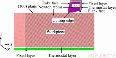
Fig. 1 Equilibrium configuration of monocrystalline Cu workpiece and diamond tool for nanomachining
At the beginning of each simulation, the tool has its thermal velocity plus a translational velocity vt (1-5 m/s). In the MD simulation process, all fixed atoms of tool are held at the specified machining speed vt. Diamond cutting tool moves along the following two stages: nanoindentation and nanocutting. The diamond cutting tool first indents downwards normally to the workpiece (100) plane with a constant speed, then after it reaches the required cutting depth (1.4 nm), it stops movement immediately and holds the position unchanged for 10 ps. Finally, the tool moves at the specified cutting speed along the  direction.
2.2 Interatomic potential
Before carrying out MD simulation of nanomachining, it is important to ensure that the used potential function gives a reliable result for the simulation. In the present work, distinct empirical energy potentials appropriate to simulate the C―C, Cu―Cu, and Cu―C bonding are employed, respectively. The interatomic actions of carbon atoms were depicted by the Tersoff potential [21], and EAM potential was used to describe the Cu―Cu interactions [22]. So far, there are no specific empirical potentials that can be used for the simulation of Cu―C bonding, like the Tersoff potential for the covalent bonding and the EAM potential for the metallic bonding. An applicable Morse type pair potential was adopted to derive the Cu―C bonding [23], which is relatively simple and computationally inexpensive compared to the EAM and Tersoff potential. The Morse type pair potential can be written as
 (1)
(1)
where r is the length of a Cu―C bond; and D, α and r0 correspond to cohesive energy, elastic modulus and atomistic distance at equilibrium, respectively. The parameters utilized in the current MD simulation are D=0.1 eV, α=1.7 -1, and r0=2.2 , which were used successfully in the nano-scale machining process [24-26].
2.3 Temperature and structure defect definition
It is informative to investigate the evolution of temperature fields and defect structures during nanomachining. For the workpiece, the conversion between kinetic energy and the temperature of each atom can be computed at each time step with the following equation:
 (2)
(2)
where n is the number of atoms; kB is the Boltzmann constant; mi, vi and Ti represent the ith atomic mass, instantaneous velocity and temperature, respectively. For the diamond tool, the temperature of the moving atoms is estimated by
 (3)
(3)
For the sake of comparing simulation results with macroscopic thermo-mechanism properties, a suitable data average algorithm should be taken. The average temperature over 5 ps of the relaxation period is taken as the temperature of each atom. Furthermore, the contribution of tool motion in the cutting direction should not be considered in the calculation of kinetic energy. However, the contribution from the angular motion of particles should be taken into account, which is normally neglected by MD simulations.
One of the most important ingredients in the atomistic simulation of nanomachining is the technology to visualize interior defects selectively. Up to now, the most common methods to identify dislocations and other lattice defects are centrosymmetry parameter (CSP) [27], slip vector [28] and atomic coordination number technique [29]. In the current simulation, the well-known visualization technique of CSP is employed to identify the defect structures in workpiece, which is less sensitive to the temperature fluctuation. In a centrosymmetric material (such as Cu or other FCC metals), each atom has pairs of equal and opposite bonds to its nearest neighbors. As the material is distorted, these bonds will change direction and/or length, but they will remain equal and opposite. If a defect is introduced nearby, however, this equal and opposite relation no longer holds for all of the nearest-neighbor pairs. The CSP for each atom is defined as follows:
 (4)
(4)
where Ri and Ri+6 are the vectors corresponding to the six pairs of opposite nearest-neighbors in the FCC lattice. By definition, the CSP is zero for an atom in a perfect FCC material under any homogeneous elastic deformation and non-zero for an atom which is near a defect such as vacancy, dislocation or free surface.
3 Simulation results
3.1 (100) surface machining
Figure 2 illustrates the MD simulations of nanometric cutting of monocrystalline Cu (100) surface at cutting distance of 7.6 nm, 15 nm and 20 nm. During the nanomachining process, the atomic Cu―C interactions between Cu (100) surface atoms and diamond tool atoms are changed from attraction force to repulsion force, as the tool indents into workpiece surface, lattices of workpiece atoms beneath as well as ahead of cutting edge radius (shear zone) are severely compressed combined with shear in the cutting direction. When the strain energy accumulated in the deformed lattice exceeds the critical value, the atoms are rearranged successively into the lattice with less strain so as to release the deformed lattice strain. Simultaneously, some defect structures, such as dislocations, are nucleated and emitted into workpiece interior. As the cutting tool moves forward, some dislocations in shear zone emit into workpiece as defect structures, while some dislocations move upwards and finally mediate from workpiece surface. Some deformed atoms move along the rake face of cutting tool as chips, similar to the traditional cutting process, and some removed atoms accumulate on the both sides of the groove. After cutting, the machined surface undergoes a relaxation period, resulting in partial elastic recovery. It can be concluded that there are three types of deformation occurring in the workpiece: plastic deformation, elastic deformation and the combination of elastic and plastic deformation. As shown in Fig. 2, both the dislocation propagation and the chip accumulation are along the <110> direction.
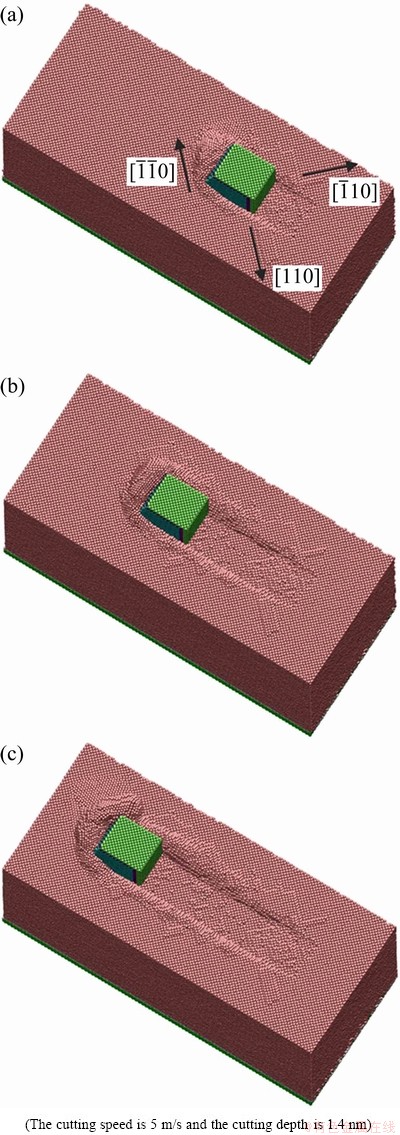
Fig. 2 MD simulation plots showing nanometric cutting of copper (100) surface at cutting distance of 7.6 nm (a), 15 nm (b) and 20 nm (c)
Figure 3 shows the variations of thrust force or normal force (Fy), cutting force (Fx) and lateral force (Fz) with cutting distance. Unlike in the traditional cutting process, the simulation results indicate that in nanometric cutting process the thrust force is larger than the cutting force. Initially, the surface atoms located in front of cutting tool and in the vicinity of cutting edge radius are suffering less deformation, the cutting force and the thrust force increase dramatically since the workpiece material is on the elastic stage. As the tool moves forward, when the accumulated local shear stress in shear zone approaches the theoretical strength of lattice, the deformed lattice strain is released by the nucleation and propagation of defect structures, which results in the fluctuation of cutting force on the diamond tool.

Fig. 3 Variation of thrust force, cutting force and lateral force with cutting distance
3.2 Temperature distribution
To understand the variation of system temperature distribution at different nanomachining stages, the central cross-sectional views and top views of system temperature distribution at cutting distance of 10.6 nm and 15 nm are selected for analysis, as shown in Fig. 4. Atoms are colored according to different system temperature ranges. It can be seen that the system temperature distribution presents a roughly concentric shape, and the highest temperature in chip is approximately 400-450 K. The temperature is about 360 K in shear zone and a relatively high temperature (~330 K) remains in the machined surface. It is worth mentioning that there is a steep temperature gradient in the cutting tool, which is much lower than in the workpiece. Compared with workpiece, the relatively smaller distance between thermostat atoms and Newton atoms enhances the temperature gradient in the cutting tool. In fact, diamond has a much higher thermal conductivity than copper and tool holder (used for installation and fixation of cutting tool) [30]. Secondly, the small volume ratio of diamond to tool holder also enhances the temperature gradient. Furthermore, from the top views of system temperature distribution, it can be seen that the atoms with higher temperature are not located in front of the tool rake face, but on the <110> direction, which is considered to be the result of dislocation nucleation and propagation as discussed in the following.

Fig. 4 Simulation results of system temperature distribution at cutting distance of 10.6 nm (a), 15 nm (b)
The defect structure nucleation and propagation during nanomachining process leads to the fluctuation of system temperature, as shown in Fig. 5, from which we can find that the average temperature in both of tool and workpiece are increased as the cutting distance increases. Initially, the temperature of tool rises rapidly and then keeps at a certain stable level. When the stress induced by the deformation of copper reaches the yield condition, the plastic deformation of workpiece would occur. The variation of system temperature can be summarized as follows. 1) The high temperature in shear zone means building up of stress in a local region. Most of heat is generated by the friction and extrusion between tool atoms and workpiece atoms. The atoms in shear zone with high temperature move forward along the rake face of cutting tool, metallic bonds are broken and bond energy is released due to plastic deformation in the workpiece. Almost all the chemical and kinetic energy are transformed into heat energy. 2) Most of heat is taken away by the chip, but the relatively small chip size and lack of energy conversion raise the system temperature ultimately. Besides, the thermostat atoms in workpiece are so far away that they can not affect the temperature of Newton atoms significantly. 3) The thermal conductivity of nanoscale particles decreases dramatically as the temperature increases, which is considered to be the result of a reduced phonon mean free path (MFP). The system temperature rises gradually with the increase of cutting length.

Fig. 5 Variations of system temperature with cutting distance in nanocutting process
3.3 Defect structure
The deformed structures in workpiece are examined to obtain a better insight into the observed temperature distribution. Prior to this study, different CSP values under various nanomachining parameters were tested, seeking an optimal CSP value to trace and identify the variation of the defect structures during the nanomachining process.
Figure 6 illustrates the defect structures at the nanoindentation depth of 0.8 nm, 1.4 nm and 1.4 nm (after relaxation for 10 ps). Atoms are colored according to the value of CSP, while the FCC atoms with the value of CSP smaller than 3.5 2 are not shown for clarity. It can be seen that stacking faults are bounded by partial dislocations. A single vacancy is formed and then more vacancies generate as the indentation depth increases. Initially, the arc-shaped cutting tool edge indents into Cu (100) surface, the dislocation loops nucleate and emit symmetrically due to the even external loading, as shown in Fig. 6(a). As the indentation depth increases, more flank face atoms of cutting tool indent into the workpiece, resulting in more defect structures nucleating and emitting. Figure 6(b) shows the defect structures at the maximum indentation depth of 1.4 nm, in which the length of dislocation loop below the tool flank face (right side) is longer than the left side due to the uneven external loading. Figure 6(c) shows the defect structures at the maximum indentation depth (1.4 nm) after relaxation for 10 ps. It can be seen that fewer defect structures and dislocation loops leave in the workpiece after relaxation, but a small dislocation loop still can be seen in the workpiece interior, which indicates that elastic recovery deformation occurs during the relaxation period. Figure 7 shows the variation of normalized principal defect structures (partial dislocation and stacking faults) in the nanoindentation stage. When the indentation depth is less than 4 (point A), no dislocation loop nucleates and emits from (100) surface into workpiece interior, which means that the local stress in the vicinity of the indentation site is far from the theoretical strength of copper and elastic deformation occurs in workpiece, and then the volume of stacking faults and partial dislocations increases as the tool moves downward, making up to 0.69% and 0.4% at the maximum indentation depth (point B). After relaxation (point C), the percentage of stacking faults and partial dislocation is reduced to 0.58% and 0.31%, respectively.
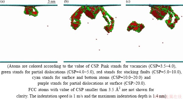
Fig. 6 Partial side views of defect structures at indentation depth of 0.8 nm (a), 1.4 nm (b) and 1.4 nm (c), after relaxation for 10 ps

Fig. 7 Statistics of normalized principle defect structures in nanoindentation stage
Figure 8 illustrates the defect structures in the workpiece at the cutting distance of 4 nm, 10.6 nm and 15 nm. Atoms are colored according to CSP values and only the surface atoms, bottom atoms and the defect-related structures are shown for clarity. From the top views of the simulation results, it can be seen that some atoms pile up in front of tool rake face as chips, while some atoms accumulate along both sides of the machined surface. When the local stress in shear zone approaches the theoretical strength of lattice, dislocations nucleate and emit away. The emission of half dislocation loops around the cutting edge intersects with the workpiece surface, making surface steps and propagating along <110> direction (top view of Fig. 8 (a)), which is the slip direction of FCC crystals. Another important phenomenon is that some atoms at the workpiece surface are shown as a bump-like pile-up in front of chips (called hillock). The hillock also emits along the <110> direction (top view of Fig. 8(b)). This similar phenomenon is in remarkably good agreement with the previous studies by FUENTE et al [31] for studying dislocation emissions during nanoindentation by scanning tunneling microscopy (STM) on Au (001) surface. The high stress field close to shear zone promotes hillocks and half dislocation loops slide away from the cutting region to interact with other defects and workpiece surface atoms. More chip atoms with high temperature are located in the  direction, since temperature increment is the function of the relative velocity of atom movement, which results in more atoms with high temperature along the dislocation emission direction.

Fig. 8 Simulation results of defect structures at cutting distance of 4.0 nm (a), 10.6 nm (b) and 15 nm (c)
The prevailing defect structures during nanocutting process are labeled by numbers as shown in Fig. 8. Number 1 stands for the V-shaped dislocations and number 2 stands for dislocation loops. The simulation results show that the V-shaped dislocations and the dislocation loops are mobile, which can be diffused into other types of defects. These two types of dislocation structures will gradually disappear with the increase of cutting distance as shown in the side view of Fig. 8(c). Number 3 and number 4 stand for single vacancy and vacancy clusters respectively. Unlike dislocation-related defects, these two types of defects are immobile, and more defect structures are nucleated as the cutting distance increases. The increasing vacancies and other types of dislocations generate and emit around shear zone, indicating that an enhanced stress field is formed in the workpiece. The enhanced stress field could be relieved by dislocation starvation in the workpiece surface, making surface steps, as shown in the top views of Figs. 8(b) and 8(c). Surface defect structures with high temperature will aggravate the localized atoms vibration and dislocation propagation. Temperature and defect structures impose a major change on the workpiece physical properties, resulting in a poor machined surface quality.
4 Discussion of temperature dependency of defect structures
In nanomachining process, the material deformation is highly localized. Some dislocations mediate from the workpiece surface, making surface steps, while others emit into the workpiece interior as defect structures. Generally, dislocation emission is a stress dependent process [32]. The local stress in the vicinity of the nucleation site must approach the theoretical strength of lattice, in the order of several GPa. Once a dislocation is nucleated and emitted, the local stress near the nucleation sites decreases by a certain amount. Then, in order to nucleate another dislocation, the local stress must become higher than before because the previous dislocations are piled up in the workpiece and assert a back stress on the critical region [33]. Since the influence of the environmental factors is not considered here, almost all the chemical and kinetic energy are transformed into heat energy. From the temperature distribution simulation results, it can be seen that the atoms with higher temperature are mainly concentrated in chip and shear zone. High temperature accelerates lattice vibration and the thermal fluctuation becomes more severe, which inevitably results in weakening the bonding force, so atoms may have enough energy to overcome the local energy barrier. It is also indicated that as the temperature increases, the material becomes “soft” during the nanomachining process, the higher temperature in shear zone results in a smaller cutting force.
In the initial nanomachining stage, the system temperature is much lower, so the dislocation nucleation and emission can be easily observed. Then, the system temperature increases remarkably as the cutting progresses, especially in chip and shear zone. At high temperature, when the dislocation has been nucleated, it does not move away at once, but hovers around shear zone [34]. KITAGAWA et al [35] found that the relation between thermally activated energy and temperature is linear. As the temperature increases, the critical stress intensity factor decreases, which means that high temperature reduces the activation barrier for dislocation nucleation and emission. As the tool moves forwards, the highly localized stress and temperature field in shear zone and chip will promote the dislocations to be emitted from the free surface, which could lead to dislocation starvation in the bulk, as shown in Fig. 8(c). As expected, few defect structures exist in the workpiece. Furthermore, when the temperature in shear zone is higher than the critical value, the material has already been plastic before removed [36]. A high machining velocity results in system temperature increasing, especially in shear zone and chip, which indicates that a relatively high machining velocity used in nanomachining results in few defect structures in the workpiece, beneficial to obtain better machined surface quality. Point defects such as single vacancy and vacancy clusters are immobile, and they are thermodynamically stable defects. However, the dislocation-related defects are thermo- dynamically unstable. As the temperature increases, these defect structures would be dissociated into point defects during the emission process. More point defects leave in the workpiece as the system temperature increases.
5 Conclusions
A series of MD simulations of nanomachining monocrystalline copper (100) surface based on a new 3D simulation model were performed. The system temperature distribution and the corresponding thermal effect on material defect structures were investigated, which brought a new aspect to understand the defect structures nucleation and propagation in the nanomachining process. The material removal mechanism was discussed, and the temperature distribution during nanomachining was simulated. The simulation results demonstrated that the system temperature distribution showed a roughly concentric shape and a steep temperature gradient was observed in diamond tool, and the highest temperature was found to be in chip. Both chip pile-up direction and dislocation emission topologies were propagated along the <110> orientation. Then, centrosymmetry parameter technique was used to monitor and elucidate defect structures in nanomachining process. It was found that stacking faults are bounded by partial dislocations. Dislocations and vacancies are the two major defect structures. In addition, the residual defect structures impose a major change on the workpiece physical properties and machined surface qualities.
Thermal effects on the nucleation and emission of defect structures during nanomachining were discussed. It was revealed that the defect structures in the workpiece are temperature dependent. The highly localized stress and temperature field in shear zone and chip reduce the activation barrier for dislocation nucleation and emission. As the tool moves forwards, dislocations are mainly mediated by the workpiece surface, while some of them are dissociated into point defects. The simulation results also indicated that a relatively high cutting speed used in nanomachining results in few defect structures in the workpiece, beneficial to obtain highly machined surface quality. Future work is needed to understand the effect of fluid or other chemical agents on the structure transformation during nanomachining processes.
References
[1] KOMANDURI R, CHANDRASEKARAN N, RAFF L M. MD simulation of nanometric cutting of single crystal aluminum―Effect of crystal orientation and direction of cutting [J]. Wear, 2000, 242: 60-88.
[2] FANG T H, WENG C I. Three-dimensional molecular dynamics analysis of processing using a pin tool on the atomic scale [J]. Nanotechnology, 2000, 11: 148-153.
[3] JEONG W P, SOO C C, HYUN C, DEUG W L. Portable nano probe for micro/nano mechanical scratching and measuring [J]. Transactions of Nonferrous Metals Society of China, 2011, 21(s1): s205-s209.
[4] TSURU T, SHIBUTANI Y. Atomistic simulation of elastic deformation and dislocation nucleation in Al under indentation-induced stress distribution[J]. Modelling Simul Mater Sci Eng, 2006, 14: 55-62.
[5] LEUNG T P, LEE W B, LU X M. Diamond turning of silicon substrates in ductile-regime [J]. J Mater Process Technol, 1998, 73: 42-48.
[6] DOYAMA M, NOZAKEI T, KOGURE Y. Cutting, compression and shear of silicon small single crystals [J]. Nucl Instrum Methods Phys Res Sect B, 1999, 153: 147-152.
[7] KIM Y S, NA K H, CHOI S O. Atomic force microscopy-based nano-lithography for nano-patterning: A molecular dynamic study [J]. J Mater Process Technol, 2004, 155: 1847-1854.
[8] CHENG K, LUO X, WARD R. Modeling and simulation of the tool wear in nanometric cutting [J]. Wear, 2003, 255: 1427-1432.
[9] PEI Q X, LU C, LEE H P. Study of materials deformation in nanometric cutting by large-scale molecular dynamics simulations [J]. Nanoscale Res Lett, 2009, 4: 444-451.
[10] PEI Q X, LU C, LEE H P. Large scale molecular dynamics study of nanometric machining of copper [J]. Comput Mater Sci, 2007, 41: 177-185.
[11] MILLER R E, SHILKROT L E, CURTIN W A. A coupled atomistics and discrete dislocation plasticity simulation of nanoindentation into single crystal thin films [J]. Acta Mater, 2004, 52: 271-284.
[12] SHIARI B, MILLER R E, KLUG D D. Multiscale simulation of material removal processes at the nanoscale [J]. J Mech Phys Solids, 2007, 55: 2384-2405.
[13] ZHU C, GUO W, YU T X, WOO C H. Radial compression of carbon nanotubes: deformation and damage, super-elasticity and super- hardness [J]. Nanotechnology, 2005, 16: 1035-1039.
[14] SHIMADA S, IKAWA N, TANAKA H, UCHIKOSHI J. Structure of micromachined surface simulated by molecular dynamics analysis [J]. Ann CIRP, 1994, 43: 51-54.
[15] MEHREZ H, CIRACI S. Yielding and fracture mechanisms of nanowires [J]. Phys Rev B, 1997, 56: 12632-12642.
[16] LIANG H Y, WOO C H, HUANG H, NGAN A H W, YU T X. Dislocation nucleation in the initial stage during nanoindentation [J]. Philos Mag, 2003, 83: 3609-3622.
[17] MULLIAH D, KENNY S D, SMITH R, SANZ-NAVARRO C F. Molecular dynamic simulations of nanoscratching of silver (100) [J]. Nanotechnology, 2004, 15: 243-249.
[18] YE Y Y, BISWAS R, MORRIS J R, BASTAWROS A, CHANDRA A.Molecular dynamics simulation of nanoscale machining of copper [J].Nanotechnology, 2003, 14: 390-396.
[19]  S. A unified formulation of the constant temperature molecular dynamics methods [J]. J Chem Phys, 1984, 81: 511-519.
[20] HOOVER W G. Canonical dynamics: Equilibrium phase-space distributions [J]. Phys Rev A, 1985, 31: 1695-1697.
[21] TERSOFF J. Modeling solid-state chemistry: Interatomic potentials for multicomponent systems [J]. Phys Rev B, 1989, 39: 5566-5568.
[22] DAW M S, BASKES M L. Embedded-atom method: Derivation and application to impurities, surfaces, and other defects in metals [J]. Phys Rev B, 1984, 29: 6443-6453.
[23] GIRIFALCO L A, WEIZER V G. Application of the Morse potential function to cubic metals [J]. Phys Rev, 1959, 114: 687-690.
[24] FANG T H, WENG C I, CHANG J G. Molecular dynamics analysis of temperature effects on nanoindentation measurement [J]. Mater Sci Eng A, 2003, 357: 7-12.
[25] MAEKAWA K, ITOH A. Friction and tool wear in nano-scale machining―A molecular dynamics approach [J]. Wear, 1995, 188: 115-122.
[26] INAMURA T, TAKEZAWA N. Atomic-scale cutting in a computer using crystal models of copper and diamond [J]. Ann CIRP, 1992, 41: 121-124.
[27] KELCHNER C L, PLIMPTON S J, HAMILTON J C. Dislocation nucleation and defect structure during surface indentation [J]. Phys Rev B, 1998, 58: 11085-11088
[28] ZIMMERMAN J A, KELCHNER C L, KLEIN P A, HAMILTON J C, FOILES S M. Surface step effects on nanoindentation [J]. Phys Rev Lett, 2001, 87: 165507-165510.
[29] LI J, van VLIET K J, ZHU T, YIP S, SURESH S. Atomistic mechanisms governing elastic limit and incipient plasticity in crystals [J]. Nature, 2002, 418: 307-310.
[30] XIA Yang, SONG Yue-qing, LIN Chen-guang, CUI Shun, FANG Zhen-zheng. Effect of carbide formers on microstructure and thermal conductivity of diamond-Cu composites for heat sink materials [J]. Transactions of Nonferrous Metals Society of China, 2009, 19(5): 1161-1166.
[31] FUENTE O R, ZIMMERMAN J A,  M A, FIGUERA J D, HAMILTON J C, PAI W W, ROJO J M. Dislocation emission around nanoindentations on a (001) fcc metal surface studied by scanning tunneling microscopy and atomistic simulations [J]. Phys Rev Lett, 2002, 88: 036101-036104.
[32] WU Hong-jun, MA Wen-hui, CHEN Xiu-hua, JIANG Yong, MEI Xiang-yang, ZHANG Cong, WU Xing-hui. Effect of thermal annealing on defects of upgraded metallurgical grade silicon [J]. Transactions of Nonferrous Metals Society of China, 2011, 21(6): 1340-1347.
[33] van VLIET K J, LI J, ZHU T, YIP S, SURESH S. Quantifying the early stages of plasticity through nanoscale experiments and simulations [J]. Phys Rev B, 2003, 67: 104105-1-15.
[34] ZHANG Y W, WANG T C, TANG Q H. The effect of thermal activation on dislocation processes at an atomistic crack tip [J]. J Phys D: Appl Phys, 1995, 28: 748-754.
[35] KITAGAWA H, NAKATANI A. Study on computational modeling for materials with crystalline structure [J]. Proc JSME A, 1993, 59: 256-262.
[36] HSIEH J Y, JU S P, LI S H, HWANG C C. Temperature dependence in nanoindentation of a metal substrate by a diamond-like tip [J]. Phys Rev B, 2004, 70: 195424-1-9.
郭永博,梁迎春
哈尔滨工业大学 机电工程学院,哈尔滨 150001
摘 要:基于建立的新型三维仿真模型,采用分子动力学方法模拟单晶铜(100)表面纳米加工过程,研究材料的去除机理和纳米加工过程中系统的温度分布与演化规律。仿真结果表明:系统的温度分布呈同心型,切屑温度最高,并且在金刚石刀具中存在较大的温度梯度。采用中心对称参数法区分工件中材料缺陷结构的形成与扩展。位错和点缺陷是纳米加工过程中工件内部的主要缺陷结构。工件中的残余缺陷结构对于工件材料的物理属性和已加工表面质量具有重要影响。位错的成核与扩展、缺陷结构的类型均与纳米加工过程中系统的温度有关。加工区域温度升高有利于位错从工件表面释放,使工件内部位错结构进一步分解为点缺陷。采用相对高的加工速度时,工件中残留缺陷结构较少,有利于获得高质量的加工表面。
关键词:单晶铜;原子尺度模拟;热效应;分子动力学模拟;纳米加工;温度分布;缺陷结构;位错;空位
(Edited by YUAN Sai-qian)
Foundation item: Project (50925521) supported by the National Natural Science Fund for Distinguished Young Scholars of China
Corresponding author: GUO Yong-bo; Tel: +86-451-86413840; Fax: +86-451-86415244; E-mail: ybguo@hit.edu.cn
DOI: 10.1016/S1003-6326(11)61530-6

