
J. Cent. South Univ. (2018) 25: 2076-2084
DOI: https://doi.org/10.1007/s11771-018-3897-2

Transmitting oscillation suppression of low-Tc SQUID TEM system based on RC serial and multi-parallel capacity snubber circuit
JI Yan-ju(����)1, LI Zong-wei(����ε)1, RONG Liang-liang(������)2, XIE Li-jun(л����)1, XIE Xiao-ming(л����)2, DU Shang-yu(������)1, LIN Jun(�־�)1, 3, WANG Yuan(��Զ)1, 3
1. College of Instrumentation and Electrical Engineering, Jilin University, Changchun 130026, China;
2. Shanghai Institute of Microsystem and Information Technology, Chinese Academy of Sciences,Shanghai 200050, China;
3. National Geography Exploration Equipment Engineering Research Center, Changchun 130026, China
 Central South University Press and Springer-Verlag GmbH Germany, part of Springer Nature 2018
Abstract: A low-temperature superconducting quantum interference device (low-Tc SQUID) can improve the depth of exploration. However, a low-Tc SQUID may lose its lock owing to oscillations in the current or the occurrence of spikes when the transmitter is switched off. If a low-Tc SQUID loses its lock, it becomes impossible for the low-Tc SQUID TEM system to function normally and stably for a long period of time. This hinders the practical use of the system. In field experiments, the transmitting current is accurately measured, the voltage overshoot and current spike data are recorded, and the gradient of the primary magnetic field at the center of the transmitting loop is calculated. After analyzing the results of field experiments, it was found that when the gradient of the primary magnetic field far exceeds the slew rate of a low-Tc SQUID, the low-Tc SQUID loses its lock. Based on the mechanisms of the transmitting oscillation, an RC serial and multi-parallel capacity snubber circuit used to suppress such oscillation is proposed. The results of simulation and field experiments show that, when using a 100 m��100 m transmitting loop, the gradient of the primary magnetic field is suppressed from 101.4 to 2.4 mT/s with a transmitting current of 40 A, and from 29.6 to 1.4 mT/s with a transmitting current of 20 A. Therefore, it can be concluded that the gradient of the primary magnetic field is below the slew rate of a low-Tc SQUID after adopting the proposed RC serial and multi-parallel capacity snubber circuit. In conclusion, the technique proposed in this paper solves the problem of a lost lock of a low-Tc SQUID, ensuring that the low-Tc SQUID TEM system functions stably for a long period of time, and providing technical assurance for ground TEM exploration at an additional depth.
Key words: low-Tc SQUID; transmitter; oscillation; snubber circuit
Cite this article as: JI Yan-ju, LI Zong-wei, RONG Liang-liang, XIE Li-jun, XIE Xiao-ming, DU Shang-yu, LIN Jun, WANG Yuan. Transmitting oscillation suppression of low-Tc SQUID TEM system based on RC serial and multi-parallel capacity snubber circuit [J]. Journal of Central South University, 2018, 25(9): 2076�C2084. DOI: https://doi.org/10.1007/s11771-018-3897-2.
1 Introduction
A low-temperature superconducting quantum interference device (low-Tc SQUID) [1, 2] has many advantages, such as a high slew rate, low noise, broad bandwidth, and linear response in the frequency band. In recent years, with the gradual maturity of low-Tc SQUID technology, applying a low-Tc SQUID to a ground TEM system has become extremely popular, as it allows a detection at depths of more than 1000 m [3, 4]. Researchers from all over the world have already tried to apply a low-Tc SQUID to TEM systems [5�C8]. In a field experiment in 2001, CHWALA et al [9] from Jena, Germany applied low-Tc SQUID to large fixed loops for the first time, using a Geonics TEM57 MK2 transmitter and ProTEM receiver. In 2014, the Shanghai Institute of Microsystem and Information Technology at the Chinese Academy of Sciences, in cooperation with Jilin University, employed a low-Tc SQUID for ground TEM detection [10].
In a TEM field experiment conducted on Hengsha Island [11], current peaks and disturbances occurred during the off-time of the transmitter current. Under such conditions, a low-Tc SQUID loses its lock and prevents the entire system from functioning stably for a long period of time. Two effective methods are presented to solve this problem. One involves increasing the slew rate of the low-Tc SQUID, and the other involves decreasing the oscillatory peaks of the transmitter current. Because the slew rate of a low-Tc SQUID is finite, exporting a stable transmitter current of high quality is key to solving the problem of a lost lock.
For TEM transmitters, hollow coils have mainly been of focus, with the application of four insulated gate bipolar transistors (IGBTs) [12] alternately turned to generate a bipolar square wave. For example, QI [13] developed transmitters based on PWM technology that can transmit a current as large as 300 A. FU et al [14] reduced the off-time using a QRC current shaping circuit. Large currents and short off-time have mainly been employed in transmitting systems designed in China. Only a few studies have focused on the peaks and disturbances existing at the positive and negative edges of the transmitter current. DENG et al [15] designed a snubber circuit based on the charge�Cdischarge clamp RCD mode, limiting the peaks of the transmitter voltage to 1200 V. NING et al [16] limited the peak of the voltage to the rated value with the help of a soft-switching technique. However, the peaks are still quite large and the stability of a low-Tc SQUID system cannot be guaranteed.
To ensure that a low-Tc SQUID operates stably and does not lose its lock, the transmitters should not focus solely on a large current and long off-time, but also on decreasing the peak value of the positive and negative edges in the switch-off waveform. In this work, after analyzing an IGBT and traditional snubber circuit, we present a new type of snubber circuit using an RC serial and multi-parallel capacity snubber structure to restrain the current peaks and disturbances. The results of a field experiment illustrate that a low-Tc SQUID system can operate stably when the newly proposed snubber circuit is applied.
2 Lost lock and reasons for its occurrence
The loss of a lock is a phenomenon occurring in sensors with a phase-locked loop (PLL) [17]. In our field experiment, we used a low-Tc SQUID system with single chip readout electronics (SCRE) in the receiving system. When we use the transmitters in hand, they may excite a significant and sharp magnetic flux. The feedback system cannot offset the variation of the magnetic flux, and thus a baseline drift occurs, which has the same characteristic as the loss of a lock in sensors with a PLL. Therefore, we call this phenomenon occurring in a low-Tc SQUID system the loss of a lock.
To study the influence of this phenomenon on the stability of a low-Tc SQUID caused by a disturbance in the transmitting current, a research group carried out a series of ground TEM field experiments. A TEM57 MK2 transmitter was used as the transmitting system, as compared to the MiniTEM transmitting system designed by Jilin University, China. During the experiment, the receiving system was set to a slew rate of 3 mT/s with a response time of 10 ��s, using a low-Tc SQUID sensor and a time-domain receiver for the purposes of comparison. With a side length of 100 m, inductance of 850 ��H, and resistance of 0.6 ��, a square coil was used as the transmitting loop. We found that when the transmitting currents were 40 and 20 A, a low-Tc SQUID lost its lock and was unable to function normally. As shown in Figure 1, a baseline drift occurred in the low-Tc SQUID output signal, leading to a serious signal distortion.
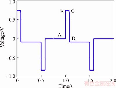
Figure 1 Baseline drift caused by low-Tc SQUID losing its lock
For a precise measurement of a TEM signal, the output voltage must change linearly, which requires an absolute value of the primary magnetic- field gradient over time that is less than the slew rate of the SQUID. At the center of the transmitting coil, the vertical component gradient over time can be approximately expressed as [18]
 (1)
(1)
where ��0 is the vacuum magnetic conductivity, L is the side length of the transmitting coil, and i(t) is the current value over time.
To calculate the central magnetic-field gradient of the transmitting coil, highly precise measurements of the transmitting current are essential. In this work, a shunt, which can be regarded as a pure resistor, is adopted. The signal sampled by the shunt is then magnified using precise amplifiers and shown on an oscilloscope with a sample rate of 4 G/s. In addition, a GPS signal is used as a trigger signal in the system. Waveforms with currents of 20 and 40 A are shown in Figures 2 and 3. As the figures indicate, the transmitting current will continuously oscillate within a few microseconds after the IGBT off-time regardless of whether the current is 20 or 40 A. The value of the peak current can be several times more than the normal current, the frequency range of which is from 500 kHz to 2 MHz.
According to Eq. (1), at the center of the transmitting coil, the primary magnetic-field gradient can be calculated. As shown in Figures 2 and 3, when the transmitting current is switched off, the maximum value of the primary magnetic-field gradient may reach 101.4 and 29.6 mT/s, respectively. Even when attenuated by the superconducting shield [19], this is still beyond 3 mT/s, which is the slew rate of a low-Tc SQUID. single chip readout electronics (SCREs) are unable to offset the variation of the magnetic flux. As a result, a baseline drift appears in the waveform. This phenomenon will lead to the SQUID losing its lock. Once such a loss occurs, the SQUID will never recover on its own.
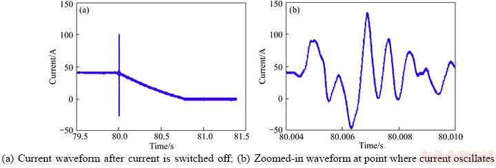
Figure 2 Transmitting current waveform at 40 A:
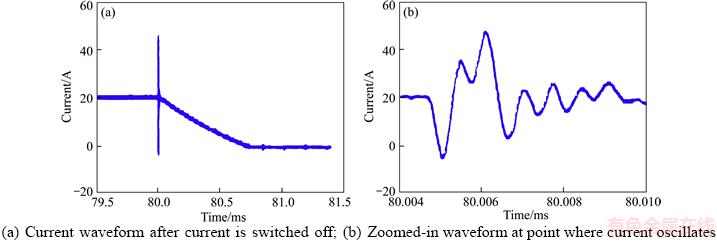
Figure 3 Transmitting current waveform at 20 A:
3 Current oscillation mechanism
Taking the MiniTEM transmitter designed by Jilin University, China as an example, the H-bridge structure of the MiniTEM is shown in Figure 4.
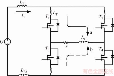
Figure 4 H-bridge structure of transmitter
Considering the equivalent physical model of wires in a transmitting system, the distributed inductance cannot be ignored. When T1 and T4 are switched off, the direction of the current in the inductive load should not abruptly change. In a circuit, T2 and T3 are FWDs, and thus the change in the direction of the current in the circuit is from a to b. The voltage between T1 and T4 can be expressed as
 (2)
(2)
where Lp=Lp1+Lp2+2LT, iL represents the current at the off-time, and Ud is the break-over voltage of the diode.
The voltage across the load is as follows:
 (3)
(3)
To study the voltage peaks between the IGBT at the off-time, the modeling and simulation are conducted based on the Multisim platform, using the same parameters as with a practical transmitting coil. The distributed capacity between the coil and ground is set at 300 pF. The results of the simulation are shown in Figure 5.
The value of di/dt is quite large because the off-time of the IGBT is always at an order of magnitude of nanoseconds. Therefore, high voltages consistently appear between the transmitting coils during the off-time. In a transmitting circuit, a distributed inductance may cause voltage peaks according to the simulation applied, which significantly harms the IGBTs. At the same time, the distributed capacitance will also cause large current oscillations with very large current peaks. To avoid the loss of a lock in a low-Tc SQUID system and ensure the stability and safety of the entire system, we must absorb both the voltage and current peaks occurring in the transmitting system. Based on the analysis above, a new type of circuit is proposed herein.
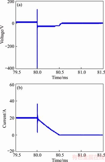
Figure 5 Voltage (a) and current spikes (b) simulated without snubber circuit
4 RC serial and multi-parallel capacity snubber circuit
As is well known, an RC snubber structure is widely used in a snubber circuit to absorb high- frequency current peaks. Traditional RC circuits possess large-value capacitors and small-value resistors, which may lead to an excessive current across the collector of the IGBT. As a result, the lifetime of the IGBT will be reduced. To suppress the current oscillation peaks and restrain the voltage and current oscillation effectively, we first propose a new type of circuit using an RC serial and multi-parallel capacity snubber circuit. The structure of the circuit is presented in Figure 6. In the circuit, C1=C2=C3=C4, R1=R2=R3=R4, C5=C6, and C7=C8. In addition, C1 through C4 mainly focus on absorbing the voltage peaks generated by IGBTs, and C5 through C8 mainly concentrate on absorbing the current peaks generated by the distributed capacitance. In this way, the consistency of the transmitting waveform can be ensured. The damping resistance RP is able to suppress the current oscillation in a late falling edge. The RC serial and multi-parallel capacity snubber circuit is greatly efficient in absorbing and improving a traditional RC absorbing circuit.
The total energy of the stray inductance in the main circuit is
 (4)
(4)
where IL represents the bus current during the off-time.
The total energy of the absorbing capacitors is
 (5)
(5)
where CT represents the total value of the absorbing capacitors in the circuit, and Upeak is an overvoltage.
At the switch-off time, the energy in the inductors is completely transferred into the capacitors. According to the energy conservation, the total value of the absorbing capacitors should be as follows:
 (6)
(6)
while taking an H-bridge with the proposed RC serial and multi-parallel capacity snubber circuit as an example, the total value of the capacitors can be expressed as follows:
 (7)
(7)
where Ipeak indicates the current peak value that an absorbing capacitor can take in.
 (8)
(8)
where CT is the value of the absorbing capacitance, and the du/dt is the maximum voltage gradient that a capacitor can have.
The capacity and maximum voltage gradient restrict each other because of a technological limitation. Capacitors with a large capacity are slow in absorbing the voltage oscillation. Although capacitors with a small capacity are sensitive in absorbing the voltage oscillation, they cannot absorb a sufficient amount of energy to meet the requirements. Therefore, to overcome these shortcomings, C1, C2, C3, and C4 should possess the following characteristics: a small capacity value, large du/dt, and the ability to withstand a high voltage. These capacitors mainly focus on absorbing the distributed inductance overvoltage in IGBTs and the current peaks. At the same time, C5 and C6 mainly aim at absorbing the distributed inductance overvoltage in the main busbar. Therefore, they should be of small capacity and low du/dt, and be able to withstand a large voltage. For C7 and C8, capacitors with a large capacity, low du/dt, and the capability to withstand a high voltage are more suitable. Gradually, the increscent capacity can help absorb more energy. According to the analysis above, the proposed RC serial and multi-parallel capacity snubber circuit are able to not only absorb oscillations with large current peaks, but also assimilate oscillations of significant amount of power.
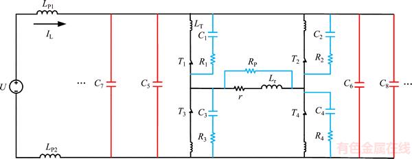
Figure 6 RC serial and multi-parallel capacity snubber circuit
A series of simulations were carried out to analyze the effects of the RC serial and multi- parallel capacity snubber circuit using the Multisim platform. The simulated voltage and current spike waveform when applying the snubber circuit are shown in Figures 7(a) and (b), respectively. The results of the overshoot voltage and peak current in the snubber circuit are presented in Table 1. The peak voltage is suppressed from 537.8 to 57.5 V, which is 11% of the original value. The peak current is restrained from 34.2 to 1.5 A, which is a 96% decrease. In conclusion, the RC serial and multi-parallel capacity snubber circuit is effective in restraining both the overshoot voltage and the peak current.
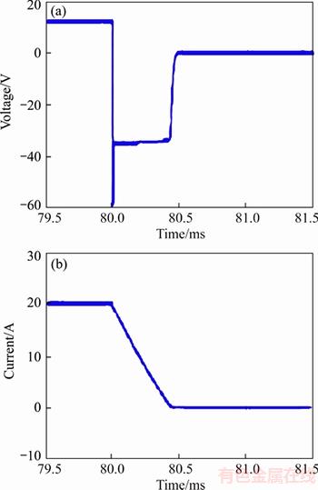
Figure 7 Voltage (a) and current (b) waveforms simulated using snubber circuit
Table 1 Simulated results using snubber circuit

5 Experiments and analysis
To verify that the snubber circuit does have a restraining effect on the actual current peaks in a transmitter, we designed a relevant RC serial and multi-parallel capacity snubber circuit matching the parameters of a SQUID TEM system. The transmitting currents were set at 20 and 40 A. According to the theoretical calculation and actual experiment, the values of the key elements are as follows: C1=0.22 ��F (2000 V), C5=1.5 ��F (1200 V), C7=450 ��F (1000V), R1=2 ��, and RP=10 ��.
To verify the effects of the snubber circuit, we conducted another field experiment on Hengsha Island using the same transmitting parameters. Hengsha Island has a very low resistivity (10�C30 ��). We used a traditional transmitter and a transmitter with the proposed RC serial and multi-parallel capacity snubber circuit separately. The base frequency was set to 0.5 Hz, and the bipolar current pulses were maintained for 80 ms. During the experiment, currents of 20 and 40 A were applied, as shown in Figure 8. Figure 8(a) shows an intact current waveform, and Figure 8(b) shows the transient waveform, during the off-time. Comparing Figures 2(b) and 8(b), we can see that the current peaks and high-frequency oscillation are prominently restrained after applying the RC serial and multi-parallel capacity snubber circuit to the transmitting system. In conclusion, this application can absorb both the current peaks and the voltage oscillations. Further, this snubber circuit can decrease electromagnetic disturbances better than a traditional circuit.
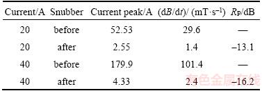
To evaluate the restraining effect, we define the peak rejection ratio as Rp=10lg(Iabs/Iori), where Iori is the current peak value in the original transmitting loop, and Iabs represents the value after applying the snubber circuit. Apparently, the lower the value of Rp is, the more outstanding the restraining effect that occurs. The actual current peak values and the corresponding Rp can be found in Table 2. After adopting the RC serial and multi-parallel capacity snubber circuit, when the current value is 20 A, Rp=�C13.1 dB with the maximum magnetic gradient value of 1.4 mT/s. When the current value is 40 A, Rp=�C16.2 dB with the maximum magnetic gradient value of 2.4 mT/s. Above all, regardless of whether the current is low or high, the maximum magnetic gradients are all less than the slew rate of the low-Tc SQUID receiving system, which guarantees that the system functions steadily for a long period of time. This is the first high-power TEM transmitter that can function steadily in a low-Tc SQUID system.
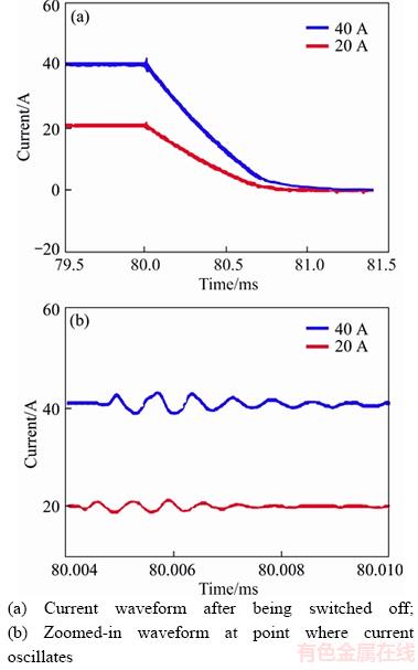
Figure 8 Current waveform with snubber circuit:
Table 2 Results of snubber effect experiments
After restraining the oscillation using the RC serial and multi-parallel capacity snubber circuit, the quality of the transmitting waveform is greatly improved. To verify the stability of a low-Tc SQUID system with the new structure, we conducted a series of field experiments where the previous experiment took place. When the transmitting current is 40 A, we recorded the output of the SQUID sensors to observe the stability over time. A 300 s output waveform is partially shown in Figure 10. The periodical impulses are the responses of the square wave step current. The swing near the zero line is the output baseline of the SQUID sensor. Figure 9 shows the details of the low-Tc SQUID output. After analyzing the waveform, we found that the phenomenon of baseline drift no longer occurs after applying the snubber circuit to the system. The tiny baseline oscillation shown in Figure 10 is caused by a secular change of the natural magnetic field. Through data processing, this tiny oscillation can be removed and will not affect the quality of the data. Figure 9 shows a portion of Figure 10. As is shown in detail in Figure 9, the baseline drift caused by a lost lock of SCRE no longer appears. When we gradually change the current within the rate current (100 A), the low-Tc SQUID system was proved through repetitive experiments to be stable for long period of time after applying the transmitter with the proposed RC serial and multi-parallel capacity snubber circuit.
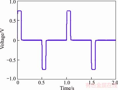
Figure 9 Details of low-Tc SQUID output
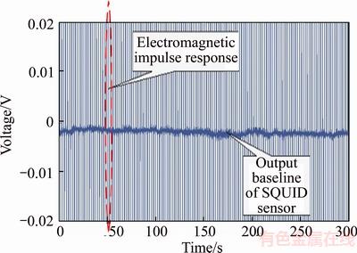
Figure 10 SQUID output signal for long time period
6 Conclusions
A lost lock is a key problem harming the stability of a low-Tc SQUID system. According to the mechanism, we proposed and simulated an RC serial and multi-parallel capacity snubber circuit, thus obtaining a way to maintain a steady state of a low-Tc SQUID system by absorbing both the current peaks and voltage oscillations. We employed the proposed RC serial and multi-parallel capacity snubber circuit in the transmitter, and conducted field experiments. According to a comparison of the current waveform and the results of the field experiments measured using different transmitters, we found that transmitters applying a RC serial and multi-parallel capacity snubber circuit provide the best results in terms of the stability of a low-Tc SQUID system. In conclusion, with a side length of 100 m and currents of 20 and 40 A, the loss of a lock no longer appears when we use transmitters with the proposed RC serial and multi-parallel capacity snubber circuit. This application still requires many improvements such as a constant voltage and linear switch-off waveform.
7 Acknowledgements
The authors would like to thank Shanghai Institute of Microsystem and Information Technology, Chinese Academy of Sciences and National Geography Exploration Equipment Engineering Research Center.
References
[1] MCCUMBER D E. Effect of AC impedance on DC voltage-current characteristics of superconductor weak-link junctions [J]. Journal of Applied Physics, 1968, 39(7): 3113�C3118.
[2] JOSEPHSON B D E. Possible new effect in superconductive tunnelling [J]. Physics Letters, 1962, 1(7): 251�C253.
[3] LESLIE K E, BINKS R A, LAM S K H, SULLIVAN P A, TILBROOK D L, THORN R G, FOLEY C P. Application of high-temperature superconductor SQUIDS for ground-based TEM [J]. The Leading Edge, 2008, 27(1): 70�C74.
[4] BICK M, PANAITOV G, WOLTERS N, ZHANG Yi, BOUSACK H, BRAGINSKI A I, KALBERKAMP U, BURKHARDT H, MATZANDER U. A HTS rf SQUID vector magnetometer for geophysical exploration [J]. IEEE Transaction on Applied Superconductivity, 1999, 9(2): 3780�C3785.
[5] STOLZ R. SQUID technology for geophysical exploration [C]// SEG Annual Meeting. New Orleans, 2006: 894�C899.
[6] PANAITOV G, BICK M, ZHANG Y, KRAUSE H J. Effect of repetitive transmitter signals on SQUID response in geophysical TEM [J]. IEEE Transactions on Applied Superconductivity, 2001, 11(1): 888�C891.
[7] ZHANG Yi, LIU Chao, SCHMELZ M, KRAUSE H J, BRAGINSKI A I, STOLZ R, XIE Xiao-ming, MEYER H G, OFFENHAUSSER A, JIANG Mian-heng. Planar SQUID magnetometer integrated with bootstrap circuitry under different bias modes [J]. Superconductor Science and Technology, 2012, 25(12): 4600�C4609.
[8] CHWALA A, STOLZ R, SCHULZ M, BAUER F, IJSSELSTEIJN R, KOSTLIN E, MEYER H G. Liquid nitrogen cooled SQUID magnetometer for TEM [C]// AAPG International Conference and Exhibition. South Africa, 2007: 26�C29.
[9] CHWALA A, SMIT J P, STOLZ R, ZAKOSARENKO V, SCHMELZ M, FRITZSCH L, BAUER F, STARKLOFF M, MEYER H G. Low temperature SQUID magnetometer systems for geophysical exploration with transient electromagnetics [J]. Superconductor Science and Technology, 2011, 24(12): 125006�C125009.
[10] CHANG Kai, ZHANG Yi, WANG Yong-liang, ZENG Jia, XU Xiao-feng, QIU Yang, KRAUSE H J, XIE Xiao-ming, OFFENHAUSSER A. A simple SQUID system with one operational amplifier as readout electronics [J]. Superconductor Science and Technology, 2014, 27(11): 115004�C115007.
[11] NABIGHIAN M N. Time-domain electromagnetic methods of exploration: Foreword and introduction [J]. Geophysics, 1984, 49(7): 849�C853.
[12] OSKUEE M R J, KARIMI M, NADERI N, RAVADANEGH S N, HOSSEINI S H. A new multilevel voltage source inverter configuration with minimum number of circuit elements [J]. Journal of Central South University, 2017, 24(4): 912�C920.
[13] QI Lin. Key technology and experiment of time-domain airborne electromagnetic transmitter [D]. Changchun: Jilin University, 2012. (in Chinese)
[14] FU Zhi-hong, ZHOU Luo-wei, SU Xiang-feng, DU Xiong. Two novel quasi-resonant steep current impulse rectifying circuits [J]. Proceedings of the CSEE, 2006, 26(5): 70�C75. (in Chinese)
[15] DENG Yi, ZHAO Zheng-ming, YUAN Li-qiang, HU Si-deng, WANG Xue-song. IGBT model for analysis of complicated multi-IGBT circuits [J]. Proceedings of CSEE, 2010, 30(9): 1�C7. (in Chinese)
[16] NING Hong-ying, SUN Xu-xia, YANG Yuan. A high-power IGBT drive protection method based on diC/dt feedback control [J]. Transactions of China Electrotechnical Society, 2015, 30(5): 33�C41. (in Chinese)
[17] CHEN Zhi-jian, CAI Min, HE Xiao-yong, XU Ken. 2.7-4GHz PLL with dual-mode auto frequency calibration for navigation system on chip [J]. Journal of Central South University, 2016, 23(9): 2242�C2253.
[18] JI Yan-ju. All-time secondary electromagnetic field extraction in high resolution transient electromagnetic system for subsurface imaging [D]. Changchun: Jilin University, 2004. (in Chinese)
[19] LIU Yang, RONG Liang-liang, JIANG Kun, CHANG Kai, KONG Xiang-yan, XIE Xiao-ming. Simulation and experimental on shielding effect of radio frequency for superconducting magnetometer [J]. Chinese Journal of Low Temperature Physics, 2014, 36(2): 136�C139. (in Chinese)
(Edited by FANG Jing-hua)
���ĵ���
���ڵ���-���ݴ����Ͷ༶���ݲ������յ�·����
low-TC SQUID TEM ϵͳ������
ժҪ��ͨ����¼�ͷ���low-Tc SQUID TEMϵͳ����������Ư�������õ���-���ݴ�����϶༶���ݲ��������յ�·�ṹ�Ż�����������Σ����ҽ�����ϵͳ���桢ʵ�ʵ�·��Լ�Ұ��ʵ����֤��������������������պ������͵�ѹ����õ����Ե����ƣ���С�����ʹ���������£�������Ȧ����һ�γ��ı仯�ʷ�ֵ��С�������õ�low-Tc SQUIDоƬ�İ��ʣ�����Ư������û���ٴγ��֣�low-Tc SQUID TEMϵͳ�ܹ���ʱ���ȶ�������
�ؼ��ʣ�low-TC SQUID��������������յ�·
Foundation item: Project(XDB 0420200) supported by Strategy Priority Research Program(B) of China
Received date: 2017-06-15; Accepted date: 2017-09-26
Corresponding author: WANG Yuan, PhD, Lecturer; Tel: +86�C13504321424; E-mail: wangyuan_ciee@jlu.edu.cn; ORCID: 0000-0001- 7851-5571