Aluminum doping and dielectric properties of silicon carbide by CVD
LI Zhi-min(李智敏), SU Xiao-lei(苏晓磊), LUO Fa(罗 发),
ZHU Dong-mei(朱冬梅), ZHOU Wan-cheng(周万城)
State Key Laboratory of Solidification Processing, Northwestern Polytechnical University, Xi’an 710072, China
Received 15 July 2007; accepted 10 September 2007
Abstract: Cubic β-SiC coating was grown onto the graphite substrate by the normal pressure chemical vapor deposition using CH3SiCl3 (MTS) as a source precursor at 1 150 ℃. But the hexagonal Al4SiC4 phase was generated in the doped process with trimethylaluminium (TMA) as the dopant. Microstructure of the deposit coating as-prepared was characterized by scanning electron microscope (SEM), which consists of spherical particles with a very dense facet structure. The real component of permittivity ε′ and dielectric loss tanδ of the coatings undoped and doped by TMA were carried out by a vector network analyzer in the microwave frequency ranges from 8.2 GHz to 12.4 GHz. The results show that both of them have low values, and doped coating has lower ε′ and tan δ than undoped one due to the existence of Al4SiC4 impurity phase, which indicates that the desired Al/SiC solid solution at 1 150 ℃ in a normal argon atmosphere is not produced.
Key words: silicon carbide; aluminum doping; dielectric properties; chemical vapour deposition
1 Introduction
Silicon carbide (SiC) is often considered the most important carbide because of many attractive properties such as great hardness and chemical resistance at high temperature. On the other hand, SiC has wide band gap, high electric mobility and high thermal conductivity. Therefore it is used in structural materials and electric devices fields at elevated temperature[1-4]. In recent years, the chemical vapor deposition (CVD) silicon carbide coating on graphite substrate is an interesting field that has been widely studied for industrial applications such as oxidation protector and diffusion barrier at high temperature[5-6], and many investigators have extensively investigated the relationships among deposition rate, deposition temperature and growth kinetics of CVD β-SiC using methyltrichlorosilane (CH3SiCl3, MTS) as a precursor material[7-10].
However, little information is available on the aluminum-doped SiC coating and its dielectric properties, especially at high frequencies for isolators and electromagnetic wave absorbing materials[11]. Presently, SiC doping can be realized by ion implantation, diffusion or in-situ doping during epitaxial growth such as chemical vapor deposition, in which the dopants can be directly incorporated into SiC. Though ion implantation has many advantages of introducing impurity atoms into SiC, a fairly high temperature annealing (1 500-1 700 ℃) is required to remove the effects of the damage and achieve reasonable electrical activation percentage of impurities[12-14]. Additionally, diffusion is thought to be unacceptable because diffusion in SiC has to be carried out at above 1 800 ℃ due to the extremely low diffusivity of impurities[15]. The aim of this work was to investigate the chemical composition, microstructure and dielectric property of silicon carbide doped by Al using CVD.
2 Experimental
Al-doped SiC coating was chemical vapor deposited on a high-purity graphite substrate at 1 150 ℃ in a normal argon atmosphere. Methytrichlorosilane (CH3SiCl3, MTS) was employed to deposit silicon carbide because it has an equivalent ratio of Si to C and a relatively low thermal decomposition temperature. Trimethylaluminum (Al(CH3)3, TMA) was used as the impurity precursor. The two source precursors were maintained at a constant temperature, respectively, and carried to the reaction chamber by bubbling hydrogen gas. Argon was used as diluent gas, which regulates the concentration of the mixture involving MTS and TMA vapors and carrier gas. The flow rates of hydrogen-to-MTS and TMA were fixed at 200 and 50 mL/min, respectively, with 100 mL/min of diluent argon.
The crystalline phase of deposited coating was examined by X-ray diffraction (XRD, X’Pert PRO MPD, Cu Kα) for crystal analysis ranging from 10? to 90? of 2θ. The surface morphology of deposited coating was observed by scanning electron microscope (SEM, JEOL JSM-6360). The samples for dielectric parameter measurement at room temperature were prepared by blending the ground coating material with paraffin in a mass ratio of 1?4, and then being molded into a 10.16 mm×22.83 mm×2 mm flange ring. The dielectric parameters were measured by a vector network analyzer (Angilent Technologies E8362B) in the frequency ranges of 8.2-12.4 GHz.
3 Results and discussion
3.1 Characterization of deposit
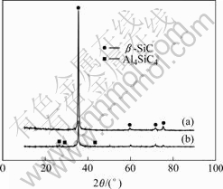
XRD patterns of the deposit coatings undoped and doped by aluminum with TMA as a precursor are shown in Fig.1. It can be seen that pure cubic type β-SiC is produced at 1 150 ℃ in a normal atmosphere without the impurity source. When doped by TMA, under the same condition, the deposit contains minor phase of the hexagonal Al4SiC4 besides cubic β-SiC. It is possible that TMA has been decomposed to Al, CH3 and CH4 with hydrogen as carrier gas before it reaches the hot reaction zone, and the MTS is pyrolyzed to generate C and SiC. So the Al4SiC4 product is generated, as shown in the following reaction[16]:
4Al+3C+SiC→Al4SiC4 (1)

Fig.1 XRD patterns of (a) undoped and (b) doped deposit coating
But it is not indicated in Fig.1 that there is the Al/SiC solid solution in the deposit due to the replacement of Si sublattice on SiC by Al. While the interplanar spacing d of β-SiC (111) peak of undoped and doped deposits is 2.525 nm and 2.526 nm, respectively, and the lattice constant a is 4.373 nm and 4.375 nm by calculating, respectively, which shows that the change of SiC lattice constant of the deposit is little after being doped. This also illustrates that Al atom does not enter possibly into the lattice of SiC deposit to change the crystal structure in the doping process.
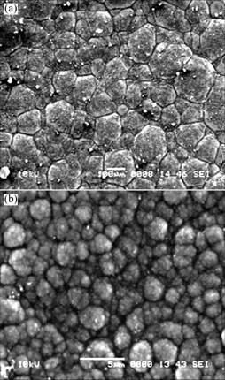
The surface morphologies of the undoped and doped coatings are shown in Fig.2. At the deposition temperature of 1 150 ℃, it is observed that both the deposited coatings have very dense facet structures, and the deposit shown in Fig.2(b) is composed of a large number of spherical particles.

Fig.2 Surface morphology of (a) undoped and (b) doped coatings
3.2 Dielectric properties of deposit
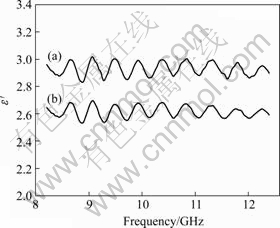
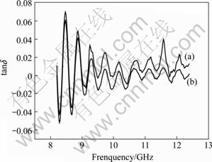
The relationship between the dielectric properties, namely the real component of permittivity ε′ and dielectric loss tanδ, and the frequency were studied for undoped and doped coatings, as shown in Figs.3 and 4, respectively. Because SiC is a non-magnetic loss material (permeability μ′=1, μ″=0), its power dissipation

Fig.3 Permittivity ε′ as function of frequency for (a) undoped and (b) doped coatings

Fig.4 Dielectric loss tanδ as function of frequency for (a) undoped and (b) doped coatings
at high frequencies is determined only by dielectric loss. Dielectric losses usually result from three primary processes: ion migration loss, including DC conductivity loss, ion jump and dipole relaxation losses, ion vibration and deformation losses, and electron polarization loss[17]. Because the β-SiC as-prepared has little defects such as VSi and VC, there hardly exists any type polarization above. So it is clear in Fig.3 that the real permittivity ε′ of both the samples is low in the frequency range of 8.2-12.4 GHz, which is slightly greater than that of pure paraffin (about 2.2). With the same batch, doped coating sample has lower ε′ than undoped one due to the Al4SiC4 impurity phase. The similar results are shown in Fig.4, and extremely low dielectric losses are obtained because the β-SiC has little dielectric loss by itself, or there hardly exists any defect polarization loss in the frequency range of 8.2-12.4 GHz. In this study, if Al atoms can substitute the site of Si on the SiC lattice to generate Al/SiC solid solution in the doped process, the electrical hole defects of SiC crystal would be produced, which will lead to the hole relaxation polarization loss in the high frequency range of 8.2-12.4 GHz, then obtain the desired or higher permittivity ε′ and dielectric loss tanδ. From the lower values of ε′ and tanδ, it is evident that there does not exist the hole defect in doped SiC crystal coating besides the impurity phase of Al4SiC4.
4 Conclusions
1) Cubic β-SiC coating is grown onto the graphite substrate by normal pressure chemical vapor deposition using MTS as a source precursor at 1 150 ℃. When the coating is doped by TMA, the hexagonal Al4SiC4 phase is generated.
2) Microstructure of the coating as-prepared consists of spherical particles with a very dense facet structure by SEM.
3) Because there hardly exists any polarization in the β-SiC as-prepared, the real permittivity ε′ of both undoped and doped samples is low in the frequency range of 8.2-12.4 GHz, which is about 2.6 and 2.9, respectively, and doped coating sample has lower ε′ than undoped one due to the presence of Al4SiC4 impurity phase. The extremely low dielectric loss tanδ of both the samples is obtained without any defect polarization loss. It is proved that the Al/SiC solid solution in the doped coating is not be produced.
References
[1] LI Zhi-min, DU Hong-liang, LIU Xiao-kui, et al. Synthesis and microwave dielectric properties of Si/C/B powders[J]. Trans Nonferrous Met Soc China, 2006, 16: s470-s473.
[2] MARTIN H P, EEKE R, MULLER E. Synthesis of nanocrystalline silicon carbide powder by carbothermal reduction[J]. Journal of European Ceramic Society, 1998, 18(12): 1737-1742.
[3] KLEIN S, WINTERER M, HAHN H. Reduced-pressure chemical vapor synthesis of nanocrystalline silicon carbide powders[J]. Chem Vap Deposition, 1998, 4(4): 143-149.
[4] MENG G W, CUI Z, ZHANG L D. Growth and characterization of nanostructured β-SiC via carbothermal reduction of SiO2 xerogels containing carbon nanoparticles[J]. Journal of Crystal Growth, 2000, 209: 801-806.
[5] XU Y, CHENG L, ZHANG L, et al. Morphology and growth mechanism of silicon carbide chemical vapor deposited at low temperatures and normal atmosphere[J]. Journal of Materials Science, 1999, 34: 551-555.
[6] LEE Young-jin, CHOI Doo-jin. The effect of diluent gases on the growth behavior of CVD SiC films with temperature[J]. Jounal of Materials Science, 2000, 35: 4519-4526.
[7] CHENG Lai-fei, XU Yong-dong, ZHANG Li-tong, et al. Oxidation and defect control of CVD SiC coating on three dimensional C/SiC composites[J]. Carbon, 2002, 40(12): 2229-2234.
[8] HALLIN C, IVANON I G, EGILSSON T, et al. The material quality of CVC-grown SiC using different carbon precursors[J]. Journal of Crystal Growth, 1998, 183: 163-174.
[9] FU Qian-gang, Li He-Jun, SHI Xiao-hong, et al. Synthesis of silicon carbide nanowires by CVD without using a metallic catalyst[J]. Materials Chemistry and Physics, 2006, 100: 108-111.
[10] WU Shou-jun, CHENG Lai-fei, ZHANG Li-tong, et al. Oxidation behavior of 2D C/SiC with a multi-layer CVD SiC coating[J]. Surface & Coatings Technology, 2006, 200: 4489-4492.
[11] ZHAO Dong-lin, ZHOU Wan-cheng. Preparation and microwave permittivity of nana Si/C/N composite powders suspended in different materials[J]. Journal of Inorganic Materials, 2001, 16(5): 909-914.(in Chinese)
[12] HEERA V, PANKNIN D, SKIRUPA W. p-Type doping of SiC by high dose Al implantation―problems and progress[J]. Applied Surface Science, 2001, 184: 307-316.
[13] GADIYAK G V. Theoretical model and computer simulation results of enhanced diffusion of high-temperature implanted aluminum in silicon carbide[J]. Nuclear Instruments and Methods in Physics Research B, 1998, 142: 313-318.
[14] PERNOT J, CAMASSEL J, CONTRERAS S, et al. Control of Al-implantation doping in 4H-SiC[J]. Materials Science and Engineering B, 2001, 80: 362-365.
[15] JANSON M S, LINARSSON M K, HALLEN A, et al. Transient enhanced diffusion of implanted boron in 4H-silicon carbide[J]. Appl Phys Lett, 2000, 76: 1434-1436.
[16] FORSBERG U, DANIELSSON ?, HENRY A, et al. Aluminum doping of epitaxial silicon carbide[J]. Journal of Crystal Growth, 2003, 253: 340-350.
[17] ZHANG Bo, LI Jin-bao, SUN Jing-ing. Solid solution of Al and N in nano-sized α-SiC powder by carbothermal reduction of the xerogels of SiO2-Al2O3[J]. Materials Letters, 2001, 51: 219-224.
(Edited by CHEN Can-hua)
Foundation item: Project (50572090) supported by the National Natural Science Foundation of China
Corresponding author: LI Zhi-min; Tel: +86-29-88488007; Fax: +86-29-88494574; E-mail: lizhmin@163.com