
Surface characterization and electrical resistivity of electroless plating nanocrystalline copper films on glass
ZHANG Hui-ping(ХЕ»бЖЅ)1, JIANG Zhong-hao(ЅЦРєЖ)1, LIAN Jian-she(Б¬ЅЁЙи)1 , HOU Xu-feng(єоРс·е)2, 3
1. Key Laboratory of Automobile Materials, Ministry of Education, College of Materials Science and Engineering, Jilin University, Changchun 130025, China;
2. Changchun Institute of Optics, Fine Mechanics and Physics, Chinese Academy of Sciences, Changchun 130033, China;
3. Graduate School, Chinese Academy of Sciences, Beijing 100039, China
Received 15 July 2007; accepted 10 September 2007
Abstract: Nanocrystalline copper films were prepared on the glass by electroless plating technique. The surface characterization of copper films with different deposition time was studied by field emission scanning electron microscopy (FESEM) and atomic force microscopy (AFM). The results indicate that the copper films have a (111) texture. A continuous and smooth film forms on the glass substrate at deposition times of 5 min. The surface roughness of as-deposited copper films becomes rougher with large nodules as the deposition time increases. According to FuchsЁCSondheimer (FЁCS), MayadasЁCShatzkes (MЁCS) theory and a combined model, the grain boundary reflection coefficient (R) is calculated in the range of 0.40-0.75. The theoretical analysis based on the experimental results show that the grain boundaries contribute mainly to the increase of electrical resistivity of nanocrystalline copper film compared with the film surfaces.
Key words: nanocrystalline copper; electroless plating; surface roughness; electrical resistivity
1 Introduction
Copper has attracted considerable attention as an alternative material to aluminum and aluminum-based alloys due to its lower resistivity and potentially higher resistance to electromigration and stress voiding for micro- and nanoscale technologies[1-5]. Copper films can be deposited by most conventional methods such as PVD and CVD. However, electrochemical methods such as electroplating[6] and electroless plating[7-10] have been proposed, alone or combined with other techniques, as candidates for fabrication of copper film. Electroless plating technique was also used to deposit a thin conformal seed layer for the subsequent electroplating process[7-10]. It has the advantages of high uniformity, good surface coverage, low tool cost, low processing temperature, high quality material and the ability to form alloys[1-3, 10]. Electroless copper plating is the result of a redox reaction between copper ions and a reducing agent both present in the same solution in a metastable state[4].
Although some studies have focused on process parameters[10], bath composition[11] and additive[12], little has been reported on the surface roughness and electrical resistivity of electroless plating copper films. In this work, electroless plating technique is used to deposit a thin copper film on the glass substrate. The microstructure, morphology, surface roughness and electrical resistivity under different deposition times were investigated.
2 Experimental
The deposition of electroless plating copper films on the glass substrate requires pretreatment. This was achieved by ultrasonic cleaning in ethanol and acetone, sensitisation in SnCl2 solution, activation in PdCl2 solution, and acceleration in HCHO solution. The bath used to obtain the electroless plating copper films consisted of 10 g/L CuSO4Ў¤5H2O, 40 g/L NaKC4H4O6, 8 g/L NaOH, 2 g/L Na2CO3, 1 g/L NiCl2Ў¤6H2O, 20 ml/L HCHO, and 0.2-0.5 g/L sodium dodecyl benzene sulfonate (SDBS). The pH value of the bath was adjusted by the NaOH solution to 12.0-12.5. The temperature of the bath was maintained at 40 Ўж with a thermoregulator and agitated by magnetic stirring. More details about this technique can be found in our previous work[13].
The crystalline structure, preferred orientation and grain size of electroless plating copper films were determined by XRD (D/max 2500PC, Rigaku, Japan), Cu K¦Б, ¦Л=0.154 056 nm. Field emission scanning electron microscope (FESEM, JSM-6700F, JEOL, Japan) and atomic force microscope (AFM, Nanoscope §єa, Veeco, USA) were used to observe the surface morphology of electroless plating copper films, while AFM was also employed to assess the surface roughness of the films. The film thickness was determined by Tangent Profilometer (Dektak 16000, Veeco, USA). The resistivity of the samples was measured by four-point probe system (Resitable-XYMCP, ST50, Mitsubishi Chemical Corporation, Japan).
3 Results and discussion
Fig.1 shows the XRD patterns of the electroless plating copper films deposited on the glass substrate for different deposition times. The strong (111) and very weak (200) reflection peaks at the deposition times of 5 min and 10 min indicate that the copper films have a texture. The I(111)/I(200) intensity ratios for different deposition times are shown in Table 1. For randomly oriented powdered copper samples, I(111)/I(200)=2.17[10]. A preferred crystal orientation of (111) is observed for the electroless plating copper films deposited more than 5 min. It can be seen that the preferred crystal orientation of (111) increases with increasing deposition time. The preferred crystal orientation of (111) is also observed in the electroless plating[10] and electroplated copper[6]. The texture of electroless copper is important as the copper film is used as seed layer for copper electro-plating in ULSI. The plated copper film will adopt he crystal orientation of the seed layer (epitaxial effect) and a highly (111) texture is preferred for better electromigration performance[10]. It is well known that copper has the face-centered-cubic (FCC) structure and (111) is the closest packed plane in FCC structure. The (111) texture is favored by the surface and interfacial energy minimization[14]. Therefore, (111) nodules coarsened during the progress of electroless plating.
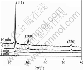
Fig.1 XRD patterns of electroless plating copper films deposited for different deposition times
The mean grain size of electroless plating copper films was calculated from the XRD results by using (111) diffraction peak according to ScherrerЎЇs equation. The mean grain size shown in Table 1 increases from 15.5 nm to 27.2 nm when the deposition time increases.
Fig.2 shows the surface morphology variation of the electroless plating copper films with deposition time. At deposition of 1 min, the film is non-uniform and some isolated nodules are observed. However, for 3 min deposition, the film is smooth and the continuous. Besides, the size of these nodules increases and coalescence of the nodules occurs. The film deposited for 5 min is continuous and shows more uniform nodule size distribution. Eventually, an extremely dense copper film is achieved after 10 min deposition. It is apparent that a
Table 1 Properties of electroless plating copper films after different deposition times

continuous copper film can be achieved at the deposition time of 5 min. Moreover, the nodule size increases during the progress of electroless plating.
Fig.3 shows the AFM pictures of electroless plating copper films on the glass with different deposition times. Figs.3(a)-(c) illustrate that the nodules size tends to
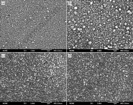
Fig.2 FESEM images of electroless plating copper films after different deposition times: (a) 1 min; (b) 3 min; (c) 5 min; (d) 10 min
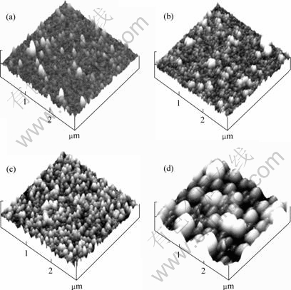
Fig.3 AFM images of electroless plating copper films after different deposition times (scan area of 3ЎБ3 ¦Мm, Z range of 50 nm): (a) 1 min; (b) 3 min; (c) 5 min; (d) 10 min
become more uniform as the film thickness increases. Meanwhile, Fig.3(d) exhibits a significant increase of nodule size with increasing film thickness. The root mean square (RMS) surface roughness of electroless plating copper films is listed in Table 1. It is apparent that the surface roughness of copper films becomes larger with large nodules as the deposition time increases. However, the surface roughness shows a little decrease at the deposition time of 10 min. This is due to the dense copper films formation resulted from the coalescence of large nodules. High uniformity in the seed layer is very important for the following electroplating copper[10]. The electric field is high at the sharp edges (peaks) of rough films, leading to the rapid plating in those regions. After electroplating, the initially non-uniform film becomes even rougher. Therefore a thin but continuous layer with low roughness and good conductivity is required.
Both the film thickness and the electrical resistivity of electroless plating copper film are also shown in Table 1. It is clearly seen that the electrical resistivity decreases with increasing film thickness. The increase of electrical resistivity in the copper film at short deposition time is probably related to the insufficient conductive path[15]. However, the experimental electrical resistivity with enough film thickness is still higher than that of bulk copper. To investigate the increase of electrical resistivity, Fuchs-Sondheimer (F-S) theory[16], Mayadas-Shatzkes (M-S) theory[17] and a combined model[18] were used to discuss the electrical resistivity of electroless copper films.
According to the F-S theory[16], the thickness dependence of the resistivity has been considered to be due to the scattering effect of conduction electrons at the film surface and interface. Based on this, the resistivity ration (¦Сs/¦С0) of the film to the bulk metal is described by
 (1)
(1)
 (2)
(2)
where ¦Сs is the film resistivity, ¦С0 is the bulk resistivity, and k (=t/¦Л0) is the ratio of film thickness (t) to the bulk mean free path (¦Л0, ¦Л0ЎЦ40 nm). The parameter p describes a fraction of the electrons scattered elastically at both the solid surface and film-substrate interface. p=0 is for dispersive surfaces and p=1 is for mirror surfaces. Simplifications to Eqn.(1) can be made as follows.
For very thin films (¦Л0)t), the approximation is given by
 (3)
(3)
For very thick films (¦Л0?t), the approximation is
 (4)
(4)
M-S theory[17] had improved the F-S theory by considering the dispersion of electrons by grain boundaries, assuming that the mean grain size, which is minor than film thickness, as the main dispersive factor. The M-S theory is expressed as
 (5)
(5)
 , R=0~1 (6)
where ¦Сg is the film resistivity including electron grain boundary scattering, D is the mean grain size, and R is the grain boundary reflection coefficient.
From the above-mentioned considerations, a combination model of F-S and M-S theory has been proposed[18]:
 ЎЎ(7)
ЎЎ(7)
where ¦Сs+g is the film resistivity including scattering effect of conduction electrons at the film surface, interface and grain scattering.
According to the method of CAMACHO et al[19], the resistivity data for electroless plating copper films were compared with the combined model and the corresponding grain boundary reflection coefficient (R) as a function of thickness obtained in Fig.4. These group of ten curves corresponds to curve from p=0 to p=1 in the arrow direction. R values are found to be in the range
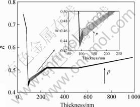
Fig.4 Grain boundary reflection coefficient (R) obtained with combined model of electrical resistivity for electroless copper film (This group of curve was calculated from p=0 (lower) to p=1 (upper) in arrow direction.)
of 0.40-0.75 in the whole thickness range. R=0.24 is reported for bulk copper in the early studies and it is much higher for copper films. Some studies have estimated that the R value is 0.4[18] and 0.46 [20] for copper film, respectively. However, CAMACHO et al[19] have reported the value of R about 0.6-0.9 for copper films.
Assuming that the total ¦С is the sum of ¦С0 (defects and phonons, etc.), the contributions of the surfaces and the grain boundaries dispersions from the combined model are calculated and shown in Fig.5. Each group of curves indicates the different values of p parameter taken from 0 to 1 in the arrow direction. Lower curves are the surface dispersions contributions and upper ones are the grain boundary contributions calculated with the grain size from the XRD results. The surface dispersions and grain boundary contributions vary with the film thickness when the film thickness is under 300 nm. However, the variation is negligible when the film thickness is over 300 nm. It is found that the electroless copper films show the most important contributions due to the grain boundaries as compared with the film surfaces. Therefore, the increasing grain boundaries are the main factor that increased the electrical resistivity in the electroless nanocrystalline copper film[20].
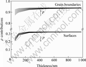
Fig.5 Main contributions of grain boundaries and surfaces for electrical resistivity determined with combined model and experimental data for electroless plating copper films
4 Conclusions
1) The electroless plating technique is an excellent tool for preparing copper film with high uniformity on the glass surface.
2) The XRD results show that (111) texture exists in the electroless nanocrystalline copper film after more than 5 min plating. The best deposition time of 5 min was determined by morphology analysis of FESEM and AFM. As the deposition time increases, the grain size and surface roughness (RMS) increase significantly, whereas the electrical resistivity decreases.
3) The calculated grain boundary reflection coefficient (R) is found to be in the range of 0.40-0.75. The increasing number of grain boundaries is the main factor that increases the electrical resistivity in the electroless nanocrystalline copper film.
References
[1] Shacham-Diamand Y, Inberg A, Sverdlov Y, et al. Electroless processes for micro- and nanoelectronics[J]. Electrochimica Acta, 2003, 48(20/22): 2987-2996.
[2] Webb E, Witt C, Andryuschenko T, et al. Integration of thin electroless copper films in copper interconnect metallization[J]. J Applied Electrochemistry, 2004, 34(3): 291-300.
[3] Shacham-Diamand Y, Dubin V M. Copper electroless deposition technology for ultra-large-scale-integration (ULSI) metallization[J]. Microelectronic Engineering, 1997, 33(1/4): 47-58.
[4] Filho S G D S, Pasa A A, Hasenack C M. A mechanism for electroless Cu plating onto Si[J]. Microelectronic Engineering, 1997, 33(1), 149-155.
[5] Goh W L, Tan K T. The use of electroless copper seed in electrochemical deposited copper interconnect[J]. Thin Solid Films, 2004, 462/463: 275-278.
[6] Teh W H, Koh L T, Chen S M, et al. Study of microstructure and resistivity evolution for electroplated copper films at near-room temperature[J]. Microelectronics Journal, 2001, 32(4): 579-585.
[7] Chong S P, Ee Y C, Chen Z, et al. Electroless copper seed layer deposition on tantalum nitride barrier film[J]. Surface &Coatings Tech, 2005, 198(1/3): 287-290.
[8] OЎЇKelly J P, Mongey K F, Gobil Y, et al. Room temperature electroless plating copper seed layer process for damascene interlevel metal structures[J]. Microelectronic Engineering, 2000, 50(1/4): 473-479.
[9] Liu R S, You C C, Tsai M S, et al. An investigation of smooth Nano-sized copper seed layers on TiN and TaSiN by new non-toxic electroless plating[J]. Solid State Communications, 2003, 125(7/8): 445-448.
[10] Ee Y C, Chen Z, Chan L, et al. Effect of processing parameters on electroless Cu seed layer properties[J]. Thin Solid Films, 2004, 462/463: 197-201.
[11] Touir R, Larhzil H, Ebntouhami M, et al. Electroless deposition of copper in acidic solutions using hypophosphite reducing agent[J]. Journal of Applied Electrochemistry, 2006, 36(1): 69-75.
[12] Lin Y M, Yen S C. Effects of additives and chelating agents on electroless copper plating[J]. Applied Surface Science, 2001, 178(1/4): 116-126.
[13] Zhang H, Jiang Z, Liu X, et al. An investigation of smooth nanosized copper films on glass substrate by improved electroless plating[J]. Surface Review and Letters, 2006, 13(4): 471-478.
[14] Lin C T, Lin K L. Effects of current density and deposition time on electrical resistivity of electroplated Cu layers[J]. J Mater Sci, 2004, 15(7): 757-762.
[15] Radoeva M, Radoev B, St?kelhuber K W. Effect of deposition inhomogeneity on the ohm resistance of thin electroless copper layers[J]. J Mater Sci, 2003, 38(12): 2703-2707.
[16] Sondheimer E H. The mean free path of electrons in metals[J]. Adv in Phys, 1952, 1(1): 1-12.
[17] Mayadas A F, Shatzkes M. Electrical-resistivity model for polycrystalline films: the case of arbitrary reflection at external surfaces[J]. Phys Rev B1, 1970, 13(2): 82-89.
[18] Lim J W, Mimura K, Isshiki M. Thickness dependence of resistivity for Cu films deposited by ion beam deposition[J]. Applied Surface Science, 2003, 217(1/4): 95-99.
[19] Camacho J M, Oliva A I. Morphology and electrical resistivity of metallic nanostructures[J]. Microelectronics Journal, 2005, 36(3/6): 555-558.
[20] Zhang W, Brongersma S H, Clarysee T, et al. Surface and grain boundary scattering studied in beveled polycrystalline thin copper films[J]. J Vac Sci Technol B, 2004, 22(4): 1830-1833.
(Edited by LONG Huai-zhong)
Foundation item: Project (2004CB619301) supported by the National Basic Research and Development Program and Project 985-Automotive Engineering of Jilin University
Corresponding author: LIAN Jian-she; Tel: +86-431-85095875; E-mail: lianjs@jlu.edu.cn