Preparation of TiO2 nanotube on glass by anodization of Ti films at room temperature
来源期刊:中国有色金属学报(英文版)2009年第1期
论文作者:汤育欣 陶杰 张焱焱 吴涛 陶海军 朱亚蓉
文章页码:192 - 198
Key words:RF magnetron sputtering; titanium films; titania nanotube; anodization
Abstract: In order to fabricate titania nanotubes on glass substrate, Ti thin films (700-900 nm) were first deposited by radio-frequency(RF) magnetron sputtering and then anodized in an aqueous HF electrolyte solution at room temperature. The morphology and structure of the nanotubes were identified by means of field emission scanning electron microscopy(FE-SEM) and X-ray diffractometry(XRD). The effects of anodization parameters (concentration of electrolyte, applied voltage) on nanotube morphology were comprehensively investigated. The results show that the dense and crystalline Ti film can be obtained on the unheated glass substrate under the sputtering power of 150 W, and the anodization current and voltage play significant roles in the formation of titania nanotube with different tube sizes.

TANG Yu-xin(汤育欣), TAO Jie(陶 杰), ZHANG Yan-yan(张焱焱),
WU Tao(吴 涛), TAO Hai-jun(陶海军), ZHU Ya-rong(朱亚蓉)
College of Material Science and Technology, Nanjing University of Aeronautics and Astronautics,
Nanjing 210016, China
Received 10 July 2008; accepted 21 October 2008
Abstract: In order to fabricate titania nanotubes on glass substrate, Ti thin films (700-900 nm) were first deposited by radio-frequency(RF) magnetron sputtering and then anodized in an aqueous HF electrolyte solution at room temperature. The morphology and structure of the nanotubes were identified by means of field emission scanning electron microscopy(FE-SEM) and X-ray diffractometry(XRD). The effects of anodization parameters (concentration of electrolyte, applied voltage) on nanotube morphology were comprehensively investigated. The results show that the dense and crystalline Ti film can be obtained on the unheated glass substrate under the sputtering power of 150 W, and the anodization current and voltage play significant roles in the formation of titania nanotube with different tube sizes.
Key words: RF magnetron sputtering; titanium films; titania nanotube; anodization
1 Introduction
Titania nanotubes have drawn extraordinary attention for their applications in photovoltaic cell[1], photocatalysis[2], sensing[3], and biomedical industry[4] due to their unique physical and chemical properties [5-7]. Many approaches such as templating synthesis, hydrothermal reactions, and anodic oxidization have been developed to prepare TiO2 nanotube. Among them the anodic oxidization is the relatively simple technique that can be easily automated to fabricate high-oriented uniform nanotube arrays. However, most of the researches focus on the anodization of titanium foils that generally have a thickness in the range from 0.1 to 2 mm. This limits the application of such a material in functional microdevices (e.g. dye-sensitized solar cells or electrochromic devices) that require a transparent metal oxide electrode[8-9].
Recently, some researchers have successfully developed the technology to grow the nanotube arrays from thin titanium films using anodization on a variety of substrates including glass[8-10], conducting glass(FTO) [11-13], and silicon[9,14-16]. Having the same electrochemical surface processes with bulk titanium foil, however, the titanium films may be rapidly etched away in acidic HF or neutral fluoride-containing solutions (forming soluble [TiF6]2- complexes) owing to high chemical dissolution rate[14]. Therefore, the quality (denseness and uniformity) of the titanium film and the following anodization parameters are critical for the formation process of titania nanotube[8,13]. According to previous studies[8-16], the substrates are normally heated to 500 ℃ to help obtain a dense, uniform titanium film suitable for anodization. And the electrolytes are kept constant at low temperature in order to decrease the chemical dissolution rate of the oxide layer formed in acidic solution. For example, MOR et al [8,11-12] have fabricated titania nanotube arrays via anodizing titanium bilayer-films (sputtered at 500 ℃) in an electrolyte containing acetic acid and hydrofluoric acid at 5 ℃. However, the investigation on both the preparation and the anodization of Ti films conducted at room temperature is seldom reported. In this work, it is found that the Ti film deposited at room temperature has poor adhesion to the substrates and is easy to peel off when immersed in the electrolyte. Therefore, it is necessary to study the denseness, surface morphology and crystal structure of Ti films deposited at room temperature by RF magnetron sputtering. Moreover, the process developed for fabricating titania nanotubes from titanium thin films at room temperature is presented, and the effect of different anodization conditions on the microstructure of the anodized thin films is investigated.
2 Experimental
Ti films (700-900 nm in thickness) were deposited by RF magnetic sputtering on glass substrate at room temperature. Target of 99.9% Ti (obtained from Tianyuan Inc., Shenzhen, China) was used as the material source. The base chamber pressure was below 7.0×10⁻⁴ Pa. Deposition was done under 0.5 Pa with argon gas flowing of 10 cm3/min, and the distance between the target and the sample was 60 mm. To remove pinhole defects in the titanium film, the specimen was cleaned by sonication in acetone, ethanol, and deionized water for 10 min, respectively. Anodization was conducted in different HF concentrations ranging from 0.1% to 1.0% (mass fraction) while the anodizing potential was kept at 10 V, and in 0.5% HF electrolyte while the potential of 5-30 V was applied, at room temperature (20 ℃) using a digital multimeter interfaced with a computer. The specimen was attached to copper rod as the working electrode. A platinum sheet (2 mm×1.5 cm) with a copper wire was used as the counter electrode. The distance between the working and counter electrodes was kept at 3 cm. After anodization, samples were immediately washed with distilled water and subsequently dried in air. The morphologies of the nanotubes were observed by means of field emission scanning electron microscope (FE-SEM; LEO-1530VP). The crystal phases of prepared samples were identified by an X-ray diffractometer (XRD; D8ADVANCE with Cu Kα radiation).
3 Results and discussion
3.1 Effect of sputtering parameters on microstructure of titanium films
In order to find out the suitable deposition parameters to fabricate dense and uniform titanium film by the RF magnetron sputtering technique, the structure of different Ti films deposited on glass was investigated. In our previous work[17], we found that the thickness of Ti films increases gradually, while the denseness of Ti films decreases obviously with the increase of sputtering pressure(pw), of which 0.5 Pa is more suitable. Substrate heating(Ts) could improve the denseness and crystallinity of the films, and also make Ti grains coarsen. The deposited titanium atoms on the substrate at low temperature have poor mobility, leading to loose structure of Ti film with small grain size. When the substrate temperature increases, the deposited atoms migrate adequately on the surface, which improves the denseness and tends to grow a crystal structure of the films. Therefore, the substrate was normally heated to 500 ℃ to create a dense, uniform, and crystal titanium film suitable for anodization[8, 13].
In this work, the structure of the titanium film deposited at room temperature is studied, and it is found that the magnetron sputtering power(Ps) has great influence on the microstructure and crystallization of the Ti films. Figs.1 and 2 show the FE-SEM images and X-ray diffraction patterns of Ti films deposited with different powers at room temperature. It is revealed that the deposited atoms have poor motility to diffuse at low temperature and adhere to the substrate surface they reach, tending to develop loose amorphous structure (Fig.1(a)) and fine grain nonhomogeneous polycrystalline structure (Fig.1(b)) under low sputtering power. The deposited atoms obtaining high energy from the increasing sputtering power can migrate easily, and may occupy the sites of titanium crystal lattice, which promotes the growth of the columnar structures (Fig.1(c)). It is found that the (002) diffraction peak becomes obvious and the columnar crystals appear when more than 150 W RF power is applied. This indicates that the Ti films prepared at low RF power of Ti target exhibit no obviously preferred orientation but have the tendency to show preferred orientation (Fig.2) when the films are deposited at high RF powers of Ti target. It is worth noting that the crystalline Ti films can be obtained on the unheated glass substrate under the sputtering power more than 150 W. However, when the power is too high (>167 W), the denseness of film decreases slightly with some holes at the grain boundaries. Titanium films deposited by RF magnetron sputtering with Ps=150 W, pw=0.5 Pa, t=0.5 h and Ts=RT (no heating) are selected to be anodized in the following experiment.
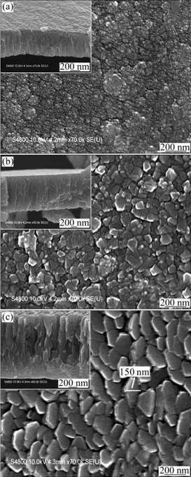
Fig.1 SEM images of Ti films deposited with different power: (a) 75 W; (b) 105 W; (c) 167 W
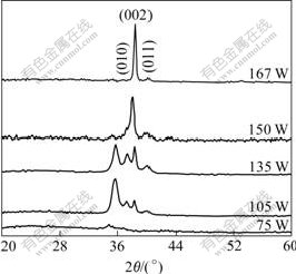
Fig.2 XRD patterns of Ti films deposited with different powers
3.2 Current/time transient at constant voltage
Fig.3 shows the typical anodization behavior of Ti thin films anodized at 10 V in 0.5% HF solution. The SEM images (Fig.4) exhibit the changes on the surface topography of the samples anodized at different times as labeled on the J―t plot. The initial current drops drastically owing to the formation of compact oxide film (about 50 nm thick[18]) on the electrolyte/metal interface at the beginning, which elevates the resistance and reduces current density. At the first step, some cracks and narrow slits appear on the surface due to the chemical and field-assistant dissolution of the oxide layer (Fig.4(a)), and then the current starts to rise owing to the reduced oxide layer thickness at this point. Fig.4(b) corresponds to the point (b) on the plot where the porous structure is formed. In this case, the pores seem to be organized and are homogeneously distributed, but the pores are covered with precipitated layer on most of the surface. Similar behavior is also observed by GONG et al[19] and MOR et al[20], which is caused by the higher amount of dissolution of Ti ions and re-precipitation of hydroxide film in HF solution. Fig.4(c) refers to the point (c), and shows that the porous oxide layer is more uniform and regular and the precipitate is less. Afterwards, the current density decays and then reaches the stable-state, which is a signal that the formation of pore reaches equilibrium with the dissolution. After anodization of 300 s, a clear self-organized nanotubular structure is formed (Fig.4(d)).
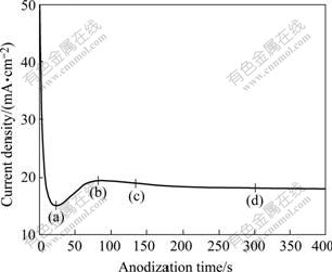
Fig.3 J―t curve of anodization of Ti films at 10 V during anodizing process in 0.5% HF solution
Fig.5 shows the surface of sample not completely anodized. Before a highly regular TiO2 nanotubular structure is established, a considerable time for compact titania oxide dissolution is required and the nanotube may be suffered from hydrous titanic oxide precipitated in HF solutions, leading to the appearance of oxide precipitate on some pore walls. It is noted that the porous film starts to form before the complete consumption of the compact oxide layer, the O2-/OH- and Ti4+ ions migrate through the oxide layer in opposite directions and eventually reach the metal/oxide interface where they react to form the dense oxide film with the help of electric field. In addition, the formation of cracks (indicated by circle) in top oxide layer can be observed. Therefore, the oxide flakes desquamate from the matrix and the porous film is exposed gradually. It is easily found that the cracks in Fig.5(b) mainly occur on original Ti grain boundaries (Fig.5(a)). It may be attributed to the irregular distribution of stress applied to the surface by the oxide layer, and the appearance of the cracks at grain boundaries is due to the higher distribution of electric field or the higher content of impurities and defects in these areas.
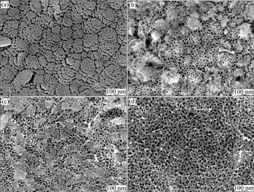
Fig.4 SEM images showing surface topography of samples anodized at different times as marked in Fig.3
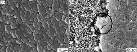
Fig.5 FE-SEM images of titanium film before anodization (a) and not completely anodized (b)
3.3 Anodization behaviors of titanium films under different anodizing conditions
In order to investigate the current transients of anodization behaviors (Fig.6) at different conditions, the samples are anodized in different HF concentrations at constant voltage (10 V) and with different applied voltages in the same HF electrolyte concentration (0.5%). The current density increases along with the increase of HF concentration (Fig.6(a)), and the current transient goes through three different processes, which is similar to Fig.6(c). It is clear that the current curve recorded is quite smooth and no fluctuation is observed when the anodization is conducted in a relatively low HF concentration (0.1%-0.5%), while current oscillations appear in a higher electrolyte concentration curve (1.0%) during the anodization process. Also, this phenomenon exists at higher voltage (25-30 V). The current oscillations are caused by passivation and repassivation, and the breakdown of the oxide layer occurs when the anodization is conducted at higher electrolyte concentration or at higher anodizing potential. When the current transient is plotted in logarithmic form (Fig.6(d), Fig.6(d)), four different slopes of current decay can be observed obviously for suitable anodization condition. For example, at the concentration of 0.5% HF with the potential range of 10-20 V and the concentration range from 0.25% to 1.0% at 10 V, while the four slopes of the other conditions cannot be distinguished easily. Typically the initial slope of the current decay curve (Figs.6(b) and (c)) is about -0.02, and the following stage of the current transient shows a slope of -0.4, 0.3 and -0.06, respectively. The different slopes of current decay presumably denote different stages of the anodic oxide layer formation. The initial shallow current decay (stage Ⅰ) in the anodization system of low HF concentration extends for a longer time compared with the system of high HF concentration in which the speed of corrosion resistant barrier layer formation is faster. Such a tendency also exists in the anodization of different voltages (Fig.4(d)). The current transients drop swiftly at the stage Ⅱ, which implies that the growth of compact oxide film is faster and the resistance rises rapidly. Moreover, the time interval of this stage is shortened obviously when the HF concentration is increased. These two slopes demonstrate the formation and growth of the barrier layer, respectively, and correspond to the initial drastic drop of current transient. Then, a slight increasing in the third stage of decaying transient (against current transient) is observed after anodization of about 15 s. This indicates that the breakdown of oxide layer starts to occur and the current rises significantly. At the fourth stage, the current begins to fall gradually owing to progressive consumption of Ti metal below the oxide barrier layer, resulting in the higher resistance as the anodization proceeds.
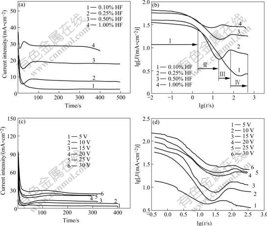
Fig.6 Current density―anodizing time curves at different conditions during anodization process: (a) Anodizing in different electrolyte concentrations ranging from 0.1% to 1.0% at 10 V; (b) Current transient of Fig.6(a) plotted in logarithmic form; (c) Anodizing in 0.5% HF solution with voltage ranging from 5 to 30 V; (d) Current transient of Fig.6(c) plotted in logarithmic form
Fig.7 shows FE-SEM images of samples anodized in 0.1%-0.5% HF concentration under 10 V and in 0.5% HF with the voltage ranging from 5 V to 30 V at RT. For a low HF concentration (Fig.7(a)) or applied voltage (Fig.7(d)), no porous structures are found except for some irregular big pits after 5 min anodization, and the crack mainly appears along the grain boundaries. This can be explained by the fact that the considerable dissolution of Ti takes place when the applied voltage or the HF concentration is low, and the fluorine ions may cause the big pits with the assistance of the applied electric field. When anodizing at relatively high concentration (0.25%, 0.5%) at 10 V, the formation of nanopores is much faster than that of the rate of field-enhanced dissolution, and the tube-like structure of titania is formed (Figs.7(b) and (c)), also at 1.0% concentration (not shown). At 5 V there is only very little pore formation observed, however, at 10 V and higher potentials clearly self-organized nanotubular layers are formed (Figs.7(c), (e) and (f)). The diameter of the tube increases significantly with the increase of potential. When the applied voltage rises to 25 V, it leads to rapid dissolution of titania, resulting in thinning and breakage of the formed nanotubes. Therefore, only a disturbed porous structure is formed at 25 V (Fig.7(g)), and the morphology is severely damaged with sponge- like structure on the surface (Fig.7(h)) when the voltage reaches 30 V. This is because the Ti―O bond undergoes polarization and is weakened, promoting dissolution of the metal oxide[20-21] at the high applied electric field. Moreover, the dissolution of titania at higher voltage indicates the field-assistant chemical dissolution of the oxide appears at the oxide/electrolyte interface. Based on the current transient of anodization curves (Fig.6) and SEM images of anodized samples (Fig.7), we can conclude that the formation of nanotube arrays relies on the suitable anodization behavior, and the anodization parameters determine the dimension of nanotube. The anodization window for successfully achieving the nanotube arrays is 10-20 V for 0.5% HF concentration and 0.25%-1.0% HF concentration at 10 V.
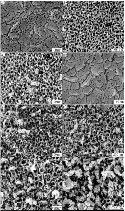
Fig.7 FE-SEM images of surface structures obtained with different electrolyte concentrations at 10 V ((a) 0.1%; (b) 0.25%; (c) 0.5%) and with different voltages in 0.5% HF solution ((d) 5 V; (e) 15 V; (f) 20 V; (g) 25 V; (h) 30 V)
4 Conclusions
The dense and crystalline Ti films were successfully obtained on the unheated glass substrate by RF magnetron sputtering under the sputtering power of 150 W. Then, nanotube titanium oxide film was prepared in an aqueous HF acidic solution at room temperature by the anodization of the titanium films.
The suitable anodization window for preparing the TiO2 nanotube arrays was 10-20 V for 0.5wt% HF concentration and 0.25wt%-1.0 wt% HF concentration at 10V at room temperature, and the microstructure of the TiO2 nanotube was dominated by the applied voltages, electrolyte concentration, and oxidation time of the anodization.
References
[1] LI D, XIA Y N. Fabrication of titania nanofibers by electrospinning [J]. Nano Lett., 2003, 3: 555-560.
[2] JANG H D, KIM S K, KIM S J. Effect of particle size and phase composition of titanium dioxide nanoparticles on the photocatalytic properties [J]. J. Nanopart. Res., 2001, 3: 141-147.
[3] VARGHESE O K, GONG D., PAULOSE M, ONG K G, GRIMES C A. Hydrogen sensing using titania nanotubes [J]. Sens. Actuators B, 2003, 93: 338-344.
[4] RODRIGUEZ R, KIM K, ONG J L, BIOMED J. In vitro osteoblast response to anodized titanium and anodized titanium followed by hydrothermal treatment [J]. Mater. Res. A, 2003, 65: 352-358.
[5] HRAPOVIC S, LUAN B L, D'AMOURS M, VATANKHAH G, JERKIEWICZ G. Morphology, chemical composition, and electrochemical characteristics of colored titanium passive layers [J]. Langmuir, 2001, 17(10): 3051-3060.
[6] VARGHESE O K, GONG D, PAULOSE M, ONG K G, DICKEY E C, GRIMES C A. Extreme changes in the electrical resistance of titania nanotubes with hydrogen exposure [J]. Adv. Mater., 2003, 15(7-8): 624-627.
[7] SCHULTZE J W, LOHRENGEL M M. Stability, reactivity and breakdown of passive films. Problems of recent and future research [J]. Electrochim. Acta, 2000, 45: 2499 -2513.
[8] MOR G K, VARGHESE O K, PAULOSE M, GRIMES C A. Transparent highly ordered TiO2 nanotube arrays via anodization of titanium thin films [J]. Adv. Funct. Mater., 2005, 15(8): 1291-1296.
[9] YU X F, LU Y X, WLODARSKI W, KANDASAMY S, KALANTAR-ZADEH K. Fabrication of nanostructured TiO2 by anodization: A comparison between electrolytes and substrates [J]. Sensors and Actuators B, 2008, 130(1):25-31.
[10] CHU S Z, INOUE S, WADA K, HISHITA S, KURASHIMA K. Self-organized nanoporous anodic titania films and ordered titania nanodots/nanorods on glass [J]. Adv. Funct. Mater., 2005, 15(8): 1343-1349.
[11] MOR G K, SHANKAR K, PAULOSE M, VARGHESE O K, GRIMES C A. Use of highly-ordered TiO2 nanotube arrays in dye-sensitized solar cells [J]. Nano Lett., 2006, 6(2): 215-218.
[12] PAULOSE M, SHANKAR K, VARGHESE O K, MOR G K, GRIMES, C A. Application of highly-ordered TiO2 nanotube-arrays in heterojunction dye-sensitized solar cells [J]. J. Phys D: Appl. Phys., 2006, 39(12): 2498-2503.
[13] LEENHEER A J, MIEDANER A, CURTIS C J, VAN HEST M F A M, GINLEY D S. Fabrication of nanoporous titania on glass and transparent conducting oxide substrates by anodization of titanium films [J]. J. Mater. Res., 2007, 22(3): 681-687.
[14] MACAK J M, TSUCHIYA H, BERGER S, BAUER S, FUJIMOTO S, SCHMUKI P. On wafer TiO2 nanotube-layer formation by anodization of Ti-films on Si [J]. Chemical Physics Letters, 2006, 428: 421-425.
[15] PREMCHAND Y D, DJENIZIAN T, VACANDIO F, KNAUTH P. Fabrication of self-organized TiO2 nanotubes from columnar titanium thin films sputtered on semiconductor surfaces [J]. Electrochemistry Communications, 2006, 8: 1840-1844.
[16] YU X F, LI Y X, GE W, YANG Q, ZHU N, ZADEH K K. Formation of nanoporous titanium oxide films on silicon substrates using an anodization process [J]. Nanotechnology, 2006, 17: 808-814.
[17] TANG Y X, TAO J, TAO H J, WU T, WANG L, ZHANG Y Y, LI Z L, TIAN X L. Fabrication and characterization for transparent electrodes of TiO2 nanotube arrays on fluorine-doped tin oxide-coated glass [J]. J. Acta Phys.-Chim. Sin., 2008, 24(6), 1120- 1126. (in chinese)
[18] BERANEK R, TSUCHIYA H, SUGISHIMA T, MACAK J M, TAVEIRA L, FUJIMOTO S, KISCH H, SCHMUKI P. Enhancement and limits of the photoelectrochemical response from anodic TiO2 nanotubes [J]. Appl. Phys. Lett., 2005, 87: 243114-243116.
[19] GONG D, GRIMES C A, VARGHESE O K, HU W, SINGH R S, CHEN Z. Titanium oxide nanotube arrays prepared by anodic oxidation [J]. J. Mater. Res., 2001, 16: 3331- 3335.
[20] MOR G K, VARGHESE O K, PAULOSE M, MUKHERJEE N, GRIMES C A. Fabrication of tapered, conical-shaped titania nanotubes [J]. J. Mater. Res., 2003, 18: 2588-2593.
[21] SUL Y T, JOHANSSON C B, JEONG Y, ALBREKTSSON T. The electrochemical oxide growth behaviour on titanium in acid and alkaline electrolytes [J]. Medical Engineering & Physics, 2001, 23: 329-346.
Corresponding author: TAO Jie, Tel: +86-25-52112900; E-mail: taojie@nuaa.edu.cn; tangyuxin008@nuaa.edu.cn
DOI: 10.1016/S1003-6326(08)60251-4
(Edited by YUAN Sai-qian)

