Fabrication of curved micro structures on photoresist layer
Jae Sung YOON, Tae-Jin JE, Doo-Sun CHOI, Sung Hwan CHANG, Kyung-Hyun WHANG
Nano Mechanical Systems Research Division, Korea Institute of Machinery and Materials (KIMM),
Daejeon 305-343, Korea
Received 21 April 2010; accepted 10 September 2010
Abstract: A novel fabrication process for micro patterns with curvature was introduced. The curved structures were made by compensating rectangular micro structures with liquid photoresist layer. Because of the surface tension of the liquid in micro scale, various shapes of meniscus can be made on the micro channels. The micro channels were made on the silicon substrate in advance, and then the liquid layer was coated on the micro channels. From the nature of liquid behavior, the curved patterns with smooth surface are obtained, which cannot be made easily with the conventional mechanical machining, as well as with the microfabrication processes, such as wet and dry etching. With this principle, it is expected that the smooth and curved surfaces can be made by simple processes and the results can be applied widely, such as optical patterns.
Key words: micro pattern; liquid layer; MEMS; micro channel; silicon substrate
1 Introduction
The microfabrication processes for MEMS have been originated from the semiconductor production techniques. However, more advanced processes have been developed with new purposes and principles. Using the photoresist layer for structural materials, rather than photo mask, is a good example for it. A lot of researchers have studied the photoresist layers for forming or etching targets. Such works have focused on the photoresist layers as pattern masters for making molding stamps of non-ferrous metals. Furthermore, various studies were conducted to control the geometries of photoresist structures, such as micro lenses and slopes [1-7]. Another approach is a study on making micro molds for forging thin non-ferrous metal films [8]. A study has focused on making slopes using light scattering during develop process [2].
The fabrication principle in this study is spin coating of photoresist onto the rectangular structures on silicon substrate, which has been made in advance with DRIE process. Similar principles have been studied with dispensing technique [9] or spray [10] of photoresist on 3 dimensional structures. However, the purpose of these studies are not to control the geometries, but to maintain uniform thickness of photoresist layer. This study focuses on the method to control the geometries of photoresist structures by changing process conditions, by which, a new geometry, different from that of mechanical or chemical machining techniques, can be obtained.
2 Experimental
2.1 Experimental setup
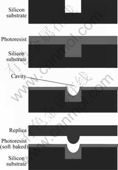
The major working principle of this study is spin coating technique of liquid photoresist onto a silicon substrate, where micro structures have been machined in advance. Fig.1 shows the schematic diagram of the fabrication process. The rectangular micro channels of 40 μm depth have been etched with DRIE process. Two kinds of channels have been made according to their widths, which are 10 μm and 100 μm, respectively, while their length is 5 mm. After preparing micro structures on the silicon wafers, the spin coating was carried out with liquid photoresist (P4620, AZ). Due to the centrifugal force of spin coating, the liquid photoresist flows toward outside of the wafer. But some of photoresist tends to remain within the channels because of the viscosity and surface tension of the liquid. Furthermore, the surface of the photoresist will be curved, or sloped because of the meniscus. After the spin coating process, the photoresist and silicon wafer were heated on a hot plate at 80 °C for 100 s so that the liquid was solidified. And the polymer replica (RepliSet-F5, Struers) was poured and spread on the photoresist surface. Then, the replicas were cut across the micro channels in order to examine the cross sections. This procedure is shown in Fig.2.

Fig.1 Schematic diagram of working process
2.2 Experimental
A major process condition in this study is the spin speed for the coating process, which affects the centrifugal force of the liquid photoresist layer. Therefore, tests were done by changing the spin speed, such as 1 000, 1 500, 2 000 and 2 500 r/min. Then, the photoresist on the silicon wafer was soft baked instantly. The soft bake process enabled the photoresist layer to be fixed, or solidified. Since the photoresist is not hard enough, a stylus profilometer cannot be used on it. So, the replica was made on top of the photoresist layer and it was cut across the channels and the cross section area was observed by an optical microscope. It was also examined that there was no diffusion or mixing between the photoresist and the replica.

Fig.2 Fabrication procedure for curved micro patterns of liquid layer
3 Results and discussion
3.1 Characteristic of 100 μm-width channel
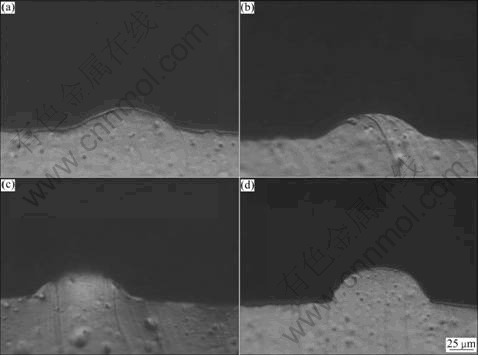
The centrifugal force increases as the spin speed increases, so the round structures of the replica in Fig.2 are expected to become large. Fig.3 shows the cross section of replica from channels with 100 μm width at various spin speeds. The bright side of the figure is the replica, so the dark side, or cavity, can be considered the photoresist layer which is upside down. The results show that there are no sharp edges on the surface because of the surface tension of the liquid, which may be a good characteristic for an optical application. The result also shows that the volume of cavity in the channel increases as the spin speeds. Accordingly, the corner is rounded more at a low speed while it becomes sharp at high speed. This means that the curvature radius of the photoresist surface becomes small and the overall thickness of the photoresist layer decreases.

Fig.3 Test results of 100 μm-width and 40 μm-depth channels at various revolution speeds: (a) 1 000 r/min; (b) 1 500 r/min; (c) 2 000 r/min; (d) 2 500 r/min
3.2 Characteristic of 10 μm-width channels
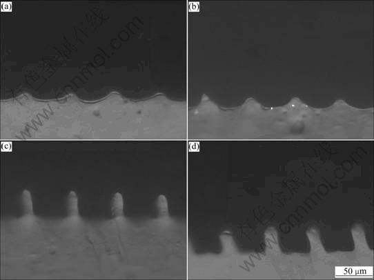
The narrower channels were also tested with the same test method. The channels with 10 μm width and 40 μm depth have higher aspect ratio. It has been well known that viscosity and surface tension become more dominant factors for fluid flow as the size decreases, and vice versa. Therefore, the photoresist in the narrower channel is expected to be hard to remove from the channels under the same condition. The spin coating was conducted at the same spin speed. Fig.4 shows the results of 10 μm-width channels at various spin speeds. As expected, a large amount of photoresist was trapped in the channels at a slow speed. And the photoresist on the neutral, or flat, area was also rounded. Consequently, the wavy patterns were fabricated at 1 000 and 1 500 r/min. From this result, it has been investigated that wavy structures, which cannot be fabricated easily with the conventional machining processes, can be formed simply because of the liquid surface tension. Furthermore, the surface roughness is expected to be favorable because it is made from the liquid surface. At faster spin speeds, the depth of the trenches increases, so that round and deep structures have been made. While the structures become more rectangular, the corners and edges are still rounded.
The structures at high speeds seem to be bent after being cut because the replica is soft and flexible while the aspect ratio is too high. Therefore, the surface geometries have been inspected with confocal laser scanning microscope (LSM5 Pascal, Carl Zeiss). Fig.5 shows the scanning results of replicas coated on the 10 μm-width channels. Since, the replicas are not cut, the original shape of the replicas can be measured. And in these tests, the surfaces are inverted so that the geometries of the photoresist layer can be observed, rather than those of the replicas. The scanning results are in good agreement with those from the optical microscope. The results also show that the geometries of the trenches are uniform along the channels, which is an important characteristic for application to industries.

Fig.4 Test results of 10 μm-width and 40 μm-depth channels at various revolution speeds: (a) 1 000 r/min; (b) 1 500 r/min; (c) 2 000 r/min; (d) 2 500 r/min

Fig.5 Surface geometries of photoresist layer on 10 μm-width and 40 μm-depth channels measured with confocal laser scanning microscope: (a) 1 000 r/min; (b) 2 500 r/min
4 Conclusions
1) This principle is a non-contact process without any tools, which can minimize surface roughness. Therefore, this process can be used for a lot of optical and microfluidic devices. And this process is also controlled by various working conditions, such as spin speed, photoresist properties and process temperature.
2) The structures of photoresist have been widely used for micro features, such as mold masters. So, the controllability of the geometries will provide wide flexibility in designing precision molds.
3) Therefore, a lot of future works are remaining, including optimization process for various fluid temperatures and properties. The precise measurement of surface roughness is required to evaluate optical characteristics. And the same process can be applied to diverse structures on substrate. For example, micro lens array can be fabricated if the photoresist is coated on the circular holes. The advanced process for larger substrate is also required for commercial application.
Acknowledgement
This study has been conducted with the support of Ministry of Knowledge and Economy through Strategic Technology Development Project and Conversing Research Center Program through the National Research Foundation of Korea (NRF) funded by the Ministry of Education, Science and Technology.
References
[1] PONOTH S S, AGARWAL N T, PERSANS P D, PLAWSKY J L. Fabrication of micromirrors with self-aligned metallization using silicon back-end-of-the-line processes [J]. Thin Solid Films, 2005, 472: 169-179.
[2] JEON J W, YOON J B, LIM K S. Sloping profile and pattern transfer to silicon by shape-controllable 3-D lithography and ICP [J]. Sensors and Actuators A, 2007, 139: 281-286.
[3] FLACK W W, FAN W P, WHITE S. The optimization and characterization of ultra-thick photoresist films [J]. SPIE Proceedings Series, 1998, 3333(2): 1288-1303.
[4] BOGDANOV A L, PEREDKOV S S. Use of SU-8 photoresist for very high aspect ratio X-ray lithography [J]. Microelectronic Engineering, 2000, 53: 493-496.
[5] SAHA S C, SAGBERG H, POPPE E, JENSEN G U, FJELDLY T A, SAETHER T. Tuning of resist slope with hard-baking parameters and release methods of extra hard photoresist for RF MEMS switches [J]. Sensors and Actuators A, 2008, 143: 452-461.
[6] SHIH T K, CHEN C F, HO J R, CHUANG F T. Fabrication of various curved relief structures through concave surface forming and soft replica molding [J]. Microelectronic Engineering, 2006, 83: 471-475.
[7] SHIH T K, CHEN C F, HO J R, CHUANG F T. Fabrication of PDMS (polydimethylsiloxane) microlens and diffuser using replica molding [J]. Microelectronic Engineering, 2006, 83: 2499-2503.
[8] JOO B Y, OH S I, SON Y K. Forming of micro channels with ultra thin metal foils [J]. CIRP Annals-Manufacturing Technology, 2004, 53(1): 243-246.
[9] KUTCHOUKOV V G, MOLLINGER J R, BOSSCHE A. New photoresist coating method for 3-D structured wafers [J]. Sensors and Actuators A, 2000, 85: 377-383.
[10] YU L, LEE Y Y, TAY F E H, ILIESCU C. Spray Coating of photoresist for 3D microstructures with different geometries [J]. J Physics: Conference Series, 2006, 34: 937-942.
(Edited by LI Yan-hong)
Corresponding author: YOON Jae-Sung, Tel: +82-42-868-7617; E-mail: jaesyoon@kimm.re.kr