
Measurement of electrical conductivity of micron-scale metallic wires
JU Bing-feng, JU Yang, M. SAKA
Department of Nanomechanics, Graduate School of Engineering, Tohoku University,
Aoba 6-6-01, Aramaki, Aoba-ku, Sendai, 980-8579, Japan
Received 10 April 2006; accepted 25 April 2006
Abstract: Electrical conductivities of micron-scale aluminum wires were quantitatively measured by a four-point atomic force microscope (AFM) probe. This technique is a combination of the principles of the four-point probe method and standard AFM. This technique was applied to the 99.999% aluminum wires with 350 nm thickness and different widths of 5.0, 25.0 and 50.0 ?m. Since the small dimensions of the wires, the geometrical effects were discussed in details. Experiment results show that the four-point AFM probe is mechanically flexible and robust. The four-point AFM probe technique is capable of measuring surface topography together with local electrical conductivity simultaneously. The repeatable measurements indicate that this technique could be used for fast in-situ electrical properties characterization of sensors and microelectromechanical system devices.
Key words: electrical conductivity; metallic wire; four-point probe; atomic force microscope
1 Introduction
The electrical properties of micron-scale metallic wires have attracted considerable attention due to their fundamental research and potential applications in fabrication of high-strength composites[1], sensors[2-4], and microelectromechanical systems (MEMS) devices [5-7]. Few of these applications are now realized in products. Majority of them, especially sensors and MEMS devices are clouded by controversy, which due to the ambiguous electrical conductivity of inside metallic interconnects; therefore, the sensors and MEMS devices are usually not functioned as expected. Though the importance of the studies has been well recognized, little was reported in literature on quantitative electrical conductivity measurement of metallic wires due to its experimental challenges.
The four-point probe method was widely applied in measuring the electrical properties of bulk solids for many decades [8, 9], in that, the electrical conductivity is measured as the ratio of current to voltage to compensate the geometrical effects. This technique is suitable for situations where the electrical conductivity is homogeneous in a volume that is large compared to the electrode spacing, but is rendered ineffective in the presence of homogeneity over smaller spacing.
In this paper, we demonstrate a four-point AFM probe technique, which is a combination of the principles of the four-point probe method and standard AFM [10]. Since the electrode spacing of the new four-point AFM probe has been minimized to be less than 1.0 mm, it allows current to flow very close to the surface, the superficial electrical conductivity measurement can be realized. By applying this new probe, the AFM not only retains the ability of surface profile imaging but also has the capability of characterizing the local electrical conductivity simultaneously.
2 Preparation of four-point AFM probe
The four-point AFM probe was fabricated based on the modification of a conventional silicon nitride bio-AFM probe with dimension of 100 μm×30 μm×0.18 μm, which is shown in Fig.1(a). A V-shaped tip with two-dimensional sliced structure was created at the tip of the cantilever. The tip height was 7.0 μm and the apex angle was less than 90?. This unique structure facilitates the microfabrication of the four electrodes. The probe was coated with 30 nm gold film and its cantilever had a spring constant around 6 pN/nm. As shown in Fig.1(b), the electrodes were introduced by fabricating three slits at the tip of the cantilever utilizing a focused ion beam system (FIB) [11]. The spacing of the two inner electrode pair (electrodes 2 and 3) is approximately 400 nm and that of the outer pair (electrode 1 and 4) is 2.4 μm. The gold film was etched to form four disconnected conducting paths. The device allows simultaneous current transmission and detection of electrical potential drop.
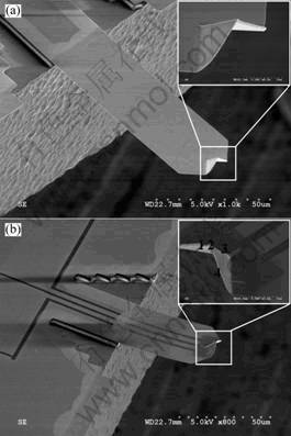
Fig.1 SEM images of four-point AFM probe: (a) Before FIB fabrication (Inset shows the original tip geometry); (b) After FIB fabrication (Inset shows details of finished four electrodes)
3 Electrical conductivity measurement
The four-point AFM probe was integrated with a multimode AFM, in which four equidistant electrodes of the four-point AFM probe were arranged as a linear array, i.e. the two outer electrodes performed as current source and drain, while the electrical potential drop was measured across the inner ones[12]. For this arrangement, there was a relationship among current I, potential drop V and conductivity σ0:
 (1)
(1)
where S1, S2 and S3 represent the ordinal spacings between electrodes. A constant current source and a voltage-preamplifier combined with a digital voltmeter were applied, which can provide the capability of current generating and voltage measuring with resolution of 50 nA and 1 nV, respectively.
The four-point AFM probe was applied to the 99.999% aluminum wires with 350 nm thickness and different widths of 5.0, 25.0 and 50.0 μm. Eqn.(1) is just fitted for a semi-infinite bulk material, but when the thickness of the thin film is smaller than the electrode spacing, the remarkable boundary effect should be taken into account[13].
4 Results and discussion
Fig.2 shows the three-dimensional AFM topography of the Al metallic wire with width of 5.0 mm (for simplicity, the same experiments for Al metallic wires with widths of 25.0 and 50.0 μm were omitted). The image presented here is generally identical with the original shape. This confirms the validation of such four-point probe to the AFM surface profile generating.
Fig.3 shows the experimental I-V relations of Al metallic wires with widths of 5.0, 25.0 and 50.0 mm, which were obtained by applying the same four-point AFM probe for the surface topography generating. The measurements were performed in the working environment of temperature 25.4 ℃, relative humidity 44.6%, with a scan rate as low as 0.5 Hz in a constant force contact mode. In order to testify the reproducibility of the four-point AFM probe, we repeated the measurements on the same spot at different contact pressures by adjusting the parameters of AFM, therefore, changed the force and contact pressure between probe and the sample surface. It is obvious that the electrical potential drop signals are clearly detected and this provides evidence that four electrodes should well scan the sample surface at the same time.
Fig.4 shows the relationship between the ratio of measured current to potential drop and that of wire thickness to electrode spacing, where w is the width of the wire and S is the minimum spacing of the electrodes
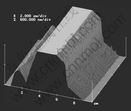
Fig.2 3D AFM image of Al metallic wire with width of 5.0 mm
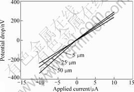
Fig.3 Typical current-voltage relationship of Al metallic wires with different widths
(i.e.S=S2=400 nm). When w is greatly larger than S (w S), the geometrical effect of w will disappear. Thus the measured I/V will not be affected by w and tend to a constant value, I0/V0, which is the same as that measured for a bulk material. Therefore, the relationship between I/V and w/S can be written as
 (2)
(2)
where a and b are positive constants. In Eqn.2, we do not consider the effect of the thickness of the wire. By considering the distribution of current in a material, we know that the effect of the thickness, t, of the wire, on the measured I/V, is similar to that of w. Therefore, Eqn.2 can be modified to
 (3)
(3)
where c and d are also positive constants. In this paper, since t is fixed to be 400 nm (the thickness of micron-scale wires is commonly fixed to a constant value in many applications), Eqn.3 can be written as
 (4)
(4)
where kt is a constant indicating the effect of t on the measured I/V. Finally, the relationship between I/V and w/S can be written as
 (5)
(5)
and
 (6)
(6)
From Eqn.5, by using three measurement data, (Ii/Vi, wi/S), i=1, 2, 3, the unknown constants K, a, and b can be determined. For simplifying the calculation, it is suggested to change the same value in w for each measurement (i.e. w3-w2=w2-w1). In this paper, although such condition is not really satisfied, an approximation is considered in order to simplify the calculation. Consequently, by using the measurement results shown in Fig.4, the constants were determined approximately as K=146.15 S (1S=1Ω-1), a=114.54 S and b=0.001. There-
fore, Eqn.5 can be expressed as
 (7)
(7)
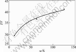
Fig.4 Relationship between ratio of measured current to potential drop and that of wire thickness to electrode spacing
Fig.5 shows the relationship between I/V and w/S obtained from Eqn.7 comparing with that obtained from the experiment. It is noted that when w/S is larger than 6000, the geometrical effect of w disappears.
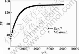
Fig.5 Relationship between I/V and w/S obtained by experiment and Eqn.7
From Eqn.1, by using the known conductivity of aluminum[14], I0/V0 was calculated to be 415.03 S. Thereby, from Eqn.6, kt was determined to be 268.88 S. Consequently, we have
 (8)
(8)
Finally, Eqn.1 can be expressed as

 (9)
(9)
From Eqn.9, for any wire with arbitrary width, by measuring I/V, the conductivity of the wire can be determined. It should be noted that if the thickness of the wire is changed, kt will also change. Therefore, a new calibration is required. By using the method described above, it is easy to determine the constants kt, a and b utilizing three reference samples.
5 Conclusions
The four-point AFM probe technique opens the way to the quantitative evaluation of micron-scale metallic wires’ electrical conductivity. The technique can self-define the boundary of the wire and facilitate the nondestructive measurement. We suggest that the technique could be used for fast in-situ electrical properties characterization of submicron interconnects widely applied in sensors and MEMS devices.
References
[1] CORSO M, AUW?RTER W, MUNTWILER M, TAMAI A, GREBER T, OSTERWALDER J. Boron nitride nanomesh[J]. Science, 2004, 303: 217-220.
[2] KONG J, FRANKLIN N R, ZHOU C, CHAPLINE M G, PENG S, CHO K, DAI H. Nanotube molecular wires as chemical sensors[J]. Science, 2000, 287: 622-625.
[3] CUI Y, WEI Q Q, PARK H K, LIEBER C M. Nanowire nanosensors for highly sensitive and selective detection of biological and chemical species[J]. Science, 2001, 293: 1289-1292.
[4] ZHENG G F, PATOLSKY F, CUI Y, WANG W U, LIEBER C M. Multiplexed electrical detection of cancer markers with nanowire sensor arrays[J]. Nat Biotechnol, 2005, 23: 1294-1301.
[5] CRAIGHEAD H G. Nanoelectromechanical systems[J]. Science, 2000, 290: 1532-1535.
[6] CARR D W, EVOY S. Measurement of mechanical resonance and losses in nanometer scale silicon wires[J]. Appl Phys Lett, 1999, 75: 920-922.
[7] ILIC B, CZAPLEWSKI D, CRAIGHEAD H G, NEUZIL P, CAMPAGNOLO C, BATT C. Mechanical resonant immunospecific biological detector[J]. Appl Phys Lett, 2000, 77: 450-452.
[8] SMITS F M. Measurement of sheet resistivities with the four-point probe[J]. Bell Syst Tech J, 1958, 37: 711-718.
[9] PETERSEN C L, HANSEN T M, B?GGILD P, BOISEN A, HANSEN O, HASSENKAM T, GREY F. Scanning microscopic four-point conductivity probes[J]. Sensor Actuat A-Phys, 2002, 96: 53-58.
[10] BINNIG G, QUATE C F, GERBER C H. Atomic force microscope[J]. Phys Rev Lett, 1986, 56: 930-933.
[11] JU Y, JU B F, SAKA M. Microscopic four-point atomic force microscope probe technique for local electrical conductivity measurement[J]. Rev Sci Instrum, 2005, 76: 086101.
[12] JU B F, JU Y, SAKA M. ?Fabrication of a microscopic four-point probe and its application to local conductivity measurement[J]. J Micromech Microeng, 2005, 15: 2277-2281.
[13] MURASHIMA S, ISHIBASHI F. Correction devisors for the four-point probe resistivity measurement on parallelepiped semiconductors[J]. Jpn J Appl Phys, 1972, 5: 685-691.
[14] VACCARI J A. Materials Handbook(15th ed)[M]. New York: McGraw-Hill, 2002.
(Edited by CHEN Wei-ping)
Foundation item: Project(17206011) supported by the Japan Society for the Promotion of Science
Corresponding author: JU Yang; Tel: +81-22-7956900; Fax: +81-795-3758; E-mail: ju@mm.mech.tohoku.ac.jp