
Grid and substrate bias effects on mechanical properties of
diamond films prepared by HFCVD
XU Feng(徐 锋)1, 2, ZUO Dun-wen(左敦稳)1, LU Wen-zhuang(卢文壮)1,
ZHU Yong-wei(朱永伟)1, WANG Min(王 珉)1
1. College of Mechanical and Electrical Engineering, Nanjing University of Aeronautics and Astronautics,
Nanjing 210016, China;
2. Nanjing Research Institute of Electronics and Technology, Nanjing 210039, China
Received 10 August 2009; accepted 15 September 2009
Abstract: Diamond films were prepared at different grid bias and substrate bias in hot filament chemical vapor deposition (HFCVD) system. The Raman and SEM results show that grain size decreases and non-diamond impurities increase for applying grid and substrate bias currents. The defects and impurities in the film increase with the decrease of grain size, which causes the decrease of hardness and elastic modulus of diamond films. The fracture toughness of film increases because of the grain size effects by applying bias. The grid bias and substrate bias make the friction coefficient smaller because of the smaller grain size and lubricating effect of graphite in the film. But the excessively high substrate bias current will lead to the dramatic decrease of mechanical properties of CVD diamond as a lot of non-diamond impurities appear in the film.
Key words: HFCVD; diamond film; grid bias; substrate bias; mechanical properties
1 Introduction
The aluminum base microwave printed circuit board (PCB) is an important device used in high frequency microwave communication fields[1]. The insulating layer of the PCB is composed of the polytetrafluoroethylene(PTFE) and ceramic powders. It is a difficult-to-machining material because of the high hardness of ceramic powder and the low heat conductivity of PTFE.
Chemical vapor deposited(CVD) diamond film is a kind of perfect cutting tool material because of its extreme hardness, low friction coefficient, excellent wear resistance and high thermal conductivity[2]. It is suitable for CVD diamond coated cutters to mill the composite material for high frequency microwave device. Hot filament CVD(HFCVD) technique is fit for the industrial synthesis of diamond coated cutters because it has low deposition cost and permits diamond deposition on substrate with complex geometry[3]. In order to obtain the smooth surface, substrate bias is often used to restrain the growth of diamond grain[4-6]. Grid bias above the filaments is added to increase the diamond nucleation density in HFCVD system[7].
The bias has obvious influence not only on the morphology but also on the mechanical properties of diamond film. But systematic studies on the effects of the substrate bias and grid bias on the mechanical properties of diamond film are less at present.
In this work, diamond films were deposited at the different grid bias and substrate bias in HFCVD system and mechanical properties including hardness, elastic modulus, fracture toughness and frictional behaviour were investigated. Research was carried out on the effects of the grid bias and substrate bias on the mechanical properties of diamond film.
2 Experimental
A double bias assisted HFCVD system was used to prepare diamond film on molybdenum substrate that had been pre-treated ultrasonically with 1 μm diamond powder suspension. The positive grid bias above the filaments and negative substrate bias were conducted to enhance the diamond nucleation. Grid bias and substrate
bias were applied in nucleation stage and grid bias was employed in growth stage. The detailed descriptions of the deposition setup and pre-treatment procedure can be found in Ref.[8].
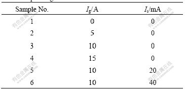
In the experiment, CH4 and H2 were used as reacting gas. Their total flow rate was about 400 mL/min, of which the CH4 gas flow rate was kept at 8 mL/min. The working pressure was kept at 2.5 kPa in the reacting chamber. The substrate bias voltage was 200-300 V and grid bias voltage was 0-100 V. The Ta filament temperature was in the range of 2 600-2 700 ℃ and the substrate temperature was about 750 ℃. Grid bias and substrate bias currents applied to the samples are listed in Table 1.
Table 1 Grid bias current (Ig) and substrate bias current (Is) used in depositing diamond film
The quality of the diamond film was evaluated by LABRAM_HR Raman spectroscopy. The light source was an argon ion laser with a wavelength of 514.5 nm. The surface morphology was determined on PHILIPS XL30 ESEM system.
Hardness and modulus of the samples were tested by nanoindentation using a MTS NanoIndenter SA2 with a diamond Berkovich indenter. Tests were performed with the maximum load of about 20 mN at a penetration depth of 20 nm. 10 points of the samples were measured for getting average hardness and elastic modulus.
The fracture toughness property of the diamond film was investigated by a MTS NanoIndenter XP which has the maximum penetration load of 500 mN. A diamond Cube-Corner indenter was used to obtain obvious radial cracks, as shown in Fig.1.
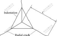
Fig.1 Radial cracks indented by Cube-Corner indenter
The fracture toughness Kc can be calculated from the radial crack length C indented by Cube-Corner indenter by the flowing equation[9]:
 (1)
(1)
where  is empirical coefficient; E is elastic modulus; H is hardness; and Pm is the maximum load of indenter.
A sliding friction experiment was conducted by diamond film in contact with a Si3N4 ball at CETR UMT tester which is shown in Fig.2.
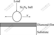
Fig.2 Schematic of slide test
3 Results and discussion
SEM images of the surface for sample No.1, No.3 and No.5 are illustrated in Fig.3. Fig.3(a) shows a typical microcrystalline diamond with a grain size of 1-2 μm. Fig.3(b) and Fig.3(c) show the smooth surfaces with the decrease of grain size. It is shown that the diamond grain size decreases with increasing grid bias current and substrate bias current. Samples No.3 and No.5 have the grain sizes of tens of nanometers.
Fig.4 shows the Raman spectra of diamond films deposited at the different grid bias currents (sample No.1-4) and substrate bias currents (sample No.5 and 6).
The peak at 1 332 cm-1 is a characteristic of diamond, which is sensitive to grain size, defects and impurities. The sp2 bonder carbon impurities usually appear at the grain boundaries of diamond[10]. It is shown in spectra of No.1-4 in Fig.4 that the diamond peaks become widened and non diamond peaks at 1 460-1 580 cm-1 are intensified with the increase of grid bias current. The grid bias currents lead to the decrease of grain size and increase of grain boundary density, which cause the increase of non diamond contents.
It is shown in spectra of No.5 and 6 in Fig.4 that the substrate bias current leads to a lot of sp2 carbon appearing in the samples. The graphite peaks are found obviously at 1 350-1 580 cm-1 while no diamond peak can be found at 1 332 cm-1 in sample No.6.

Fig.3 SEM images of surface for sample No.1 (a), No.3 (b) and No.5 (c)
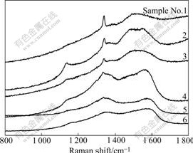
Fig.4 Raman spectra of samples at different grid bias current and substrate bias current (Laser wavelength 514.5 nm)
Fig.5 shows the nanoindentation results of sample No.2. The maximum displacement of the diamond indenter is less than one tenth of the film thickness to minimize the substrate effects[11]. The method of
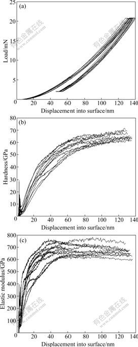
Fig.5 Load―indentation depth curves (a), hardness―depth curves (b) and elastic modulus―depth curves (c) at different positions of diamond film (sample No.2)
OLIVER-PHARR was used to evaluate the hardness and elastic modulus with the load versus displacement curves in complete load/unload cycles by assuming a Poisson ratio of 0.25.
It is shown in Fig.5 that sample No.2 has an average hardness of 58 GPa and an average elastic modulus of 680 GPa obtained from their stable indentation stage.
Fig.6 and Fig.7 show the effects of grid bias current and substrate bias current on hardness and elastic modulus of the samples.
It is shown in Fig.6 that hardness and elastic modulus decrease with increasing grid bias current. The substrate bias has obvious influence on the mechanical performance of diamond film. It leads to the dramatic decline of hardness and elastic modules as shown in Fig.7. The sample No.6 has an average hardness of 22 GPa and an average elastic modulus of 260 GPa, which is close to the level of DLC film[12].
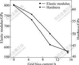
Fig.6 Effect of grid bias current on hardness and elastic modulus of sample No.1-4

Fig.7 Effect of substrate bias current on hardness and elastic modulus of sample No.4-6
Natural diamond has an hardness of 50-100 GPa and elastic modulus of 1 050 GPa[13]. The hardness and elastic modulus of CVD diamond are obvious less than those of natural diamond because of its polycrystalline structure and non-diamond impurity.
Strictly speaking, CVD diamond film has the phases of diamond and graphite. The overall hardness and modulus of the CVD diamond should be the values between those of diamond and graphite.
It is shown from the Raman spectra that the non-diamond contents increase with the increase of grid bias current and substrate bias current. This impacts the degree of amorphous carbon extending into some of the grain boundaries. The decrease of grain size leads to the increase of atoms expected to be in grain boundary environments with broken bonds, hydrogen termination, amorphous regions and sp2 bonded carbon[11-12]. It is the non-diamond impurities and defects in grain boundaries that weaken the ability to resist elastic and plastic deformation of diamond film.
Fig.8 shows the indentation SEM images of sample No.3 (Fig.8(a)) and No.5 (Fig.8(b)). In Fig.8(a), radial cracks are observed and the fracture toughness, Kc is about 6.0 MPa・m1/2 calculated by Eq.(1). It is obviously less than that of the natural diamond. No obvious cracks are found in sample No.5 as shown in Fig.8(b). The indentation is bigger than that of sample No.3 because of its low hardness.
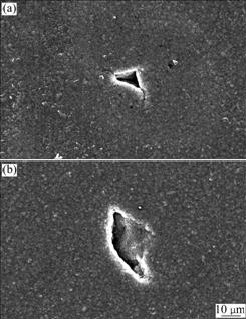
Fig.8 Indentation images of sample No.3 (a) and No.5 (b)
High level of internal compressive stress is found in the diamond film by bias action[14-15]. Owing to the compressive residual stresses and grains boundaries, fracture toughness of CVD diamond film is much higher than that of natural diamond. The defects on boundaries and fine crystalline structure make the direction of cracks change in its propagation procedure as shown in Fig.8(a).
The dependence of the friction coefficient on slide time is shown in Fig.9. It is shown that the friction coefficients keep constant after initial 60 s.
As shown in Fig.3, the grid bias and substrate bias make the surface of diamond film smoother. It is shown in Fig.9 that the friction coefficient decreases with increasing grid bias current. The friction coefficient of sample No.3 or No.5 is equal to or less than 0.1. The substrate bias current make the friction coefficient smaller because of the smaller grain size and lubricating effect of graphite in the film.
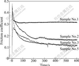
Fig.9 Friction coefficient dependent on slide time for diamond film sample No. 1, 2, 3 and 5
4 Conclusions
1) In HFCVD system, grid bias current and substrate bias current lead to the decrease of grain size and the increase of grain boundary and crystal defects in diamond film.
2) Hardness and elastic modulus of diamond film decrease with the increase of grid bias current and substrate bias current.
3) The fracture toughness increases because of the small diamond grain size by applying grid bias. The substrate and grid bias currents make the friction coefficient smaller for the smaller grain size and lubricating effect of graphite in the film.
4) The excessively high substrate bias current will lead to the dramatic decrease of mechanical properties.
References
[1] ZHANG Wei-ming, HAO Ming-hui, SHEN Ying-ying, ZHAO Xin. Experiment research on cutting force in process of high speed milling of the microwave printed circuit board [J]. Mechatronics, 2004(4): 15-18. (in Chinese)
[2] DAVIS R F. Diamond films and coatings: Development, properties, and applications [M]. New Jersey: Noyes Publications, 1993.
[3] XU Feng, ZUO Dun-wen, LU Wen-zhuang, WANG Min, LI Lei. FEM simulation on the 3-D temperature distribution of large area hot filament chemical vapor deposition system [J]. Chinese Journal of Mechanical Engineering, 2007, 43(6): 21-25. (in Chinese)
[4] SNCHEZ G, WANG W L, POLO M C, ESTEVE J. Nucleation of diamond on silicon by biased HFCVD: A comparative study [J]. Diamond and Related Materials, 1998, 7: 200-204.
[5] JIANG X, ZHANG W J, KLAGES C P. Effects of ion bombardment on the nucleation and growth of diamond films [J]. Physical Review B, 1998, 58: 7064-7075.
[6] YUGO S. Generation of diamond nuclei by electric field on nondiamond substrates for electronic application [J]. Applied Physics Letter, 1991, 58: 1036-1040.
[7] XU Feng, ZUO Dun-wen, LU Wen-zhuang, MANG Min. Effect of grid bias on the deposition of nanocrystalline diamond films [J]. Transaction of Nanjing University of Aeronautics and Astronautics, 2007, 24(4): 317-322.
[8] XU Feng, ZUO Dun-wen, LU Wen-zhuang, LI Xiang-feng, XIANG Bin-kun, WANG Min. Preparation of nano-crystalline diamond films on molybdenum substrate by double bias method [J]. Key Engineering Materials, 2006, 315/316: 646-670.
[9] PHARR G M. Measurement of mechanical property by ultra low load indention [J]. Mater Sci Eng A, 1998, 253(1/2): 151-159.
[10] MAYP W, SMITH J A, MANKELEVICH Y A. Deposition of NCD films using hot filament CVD and Ar/CH4/H2 gas mixtures [J]. Diamond and Related Materials, 2006, 15: 345-352.
[11] Wiora M, Brühne K, Fl?ter A, Gluche P, Willey T M, Kucheyev S O, Buuren A W, Hamza A.V, Biener J, Fecht H J. Grain size dependent mechanical properties of nanocrystalline diamond films grown by hot filament CVD [J]. Diamond and Related Materials, 2009, 18: 927-930.
[12] Philip J, Hess P, Feygelson T, Butler J E, Chattopadhyay S, Chen K H, Chen L C. Elastic, mechanical, and thermal properties of nanocrystalline diamond films [J]. Journal of Applied Physics, 2003, 93(4): 2164-2171.
[13] CHIU C C, LIOU Y, JUANG Y D. Elastic modulus and residual stresses in diamond films [J]. Thin Solid Film, 1995, 260: 118-123.
[14] XU Feng, ZUO Dun-wen, LU Wen-zhuang, WANG Min, ZHANG Hai-yu. Study of thermal stress and instrinsic stress of large area diamond thick film prepared by HFCVD [J]. Key Engineering Materials, 2008, 375/376: 123-127.
[15] NOVIKOV N V, DUB S N. Hardness and fracture toughness of CVD diamond film [J]. Diamond and Related Materials, 1996, 5: 1026-1030.
(Edited by YANG Bing)
Foundation item: Project(0802025B) supported by Jiangsu Provincial Postdoctoral Science Foundation, China; Project(BK2008382) supported by Natural Science Foundation of Jiangsu Province, China
Corresponding author: XU Feng; Tel: +86-25-84891686; E-mail: xufeng@nuaa.edu.cn