J. Cent. South Univ. Technol. (2010) 17: 1011-1020
DOI: 10.1007/s11771-010-0592-3

Design of logic process based low-power 512-bit EEPROM for UHF RFID tag chip
JIN Li-yan(金丽妍), LEE J H, HA P B, KIM Y H
Department of Electronic Engineering, Changwon National University, Changwon 641-773, Korea
? Central South University Press and Springer-Verlag Berlin Heidelberg 2010
Abstract: A 512-bit EEPROM IP was designed by using just logic process based devices. To limit the voltages of the devices within 5.5 V, EEPROM core circuits, control gate (CG) and tunnel gate (TG) driving circuits, DC-DC converters: positive pumping voltage (VPP=4.75 V), negative pumping voltage (VNN=-4.75 V), and VNNL(=VNN/2) generation circuit were proposed. In addition, switching powers CG high voltage (CG_HV), CG low voltage (CG_LV), TG high voltage (TG_HV), TG low voltage (TG_LV), VNNL_CG and VNNL_TG switching circuit were supplied for the CG and TG driving circuit. Furthermore, a sequential pumping scheme and a new ring oscillator with a dual oscillation period were proposed. To reduce a power consumption of EEPROM in the write mode, the reference voltages VREF_VPP for VPP and VREE_VNN for VNN were used by dividing VDD (1.2 V) supply voltage supplied from the analog block in stead of removing the reference voltage generators. A voltage level detector using a capacitive divider as a low-power DC-DC converter design technique was proposed. The result shows that the power dissipation is 0.34 ?W in the read mode, 13.76 ?W in the program mode, and 13.66 ?W in the erase mode.
Key words: electrically erasable programmable read-only memory (EEPROM); logic process; DC-DC converter; ring oscillator; sequential pumping scheme; dual oscillation period; radio frequency identification (RFID)
1 Introduction
Radio frequency identification (RFID) is a technology that provides various communication services among objects by collecting, storing, and revising information based on installed or attached RFID tags. Currently, passive RFID tags are more widely used than their active counterparts because they have advantages such as low-cost and smaller-sized tags. Therefore, more efforts have been devoted to the development of the passive tags.
A passive ultra-high frequency (UHF) RFID tag comprises of antenna and a tag chip. The tag chip consists of analog, logic, and memory blocks [1]. The analog block consists of a modulator, a demodulator, and a voltage multiplier, making the energy received from the antenna to a supply voltage. The logic block deals with the protocol, performs cyclic redundancy checks (CRCs), detect errors, and controls operational modes of the analog block. Electrically erasable programmable read-only memory (EEPROM) is usually used as the memory block since it has the capacity to read and write, and it can also retain stored information at power-down. The required minimum memory capacity is 512 bits.
The RFID tag chip is essential to use a low power supply since it can recognize an identification (ID) with a power supply voltage generated from the voltage multiplier of the analog block when an UHF signal is received, and it can transmit its data to a reader with the power [2-10]. In addition, it requires a low-area design to reduce its cost [11-13]. Furthermore, it is necessary to design an EEPROM IP based on a logic process without any additional EEPROM processes [5]. It also requires a circuit design technique to avoid low VDD (1.2 V supply voltage) alarms through a current surge control in entering the write mode [9].
In this work, a 512-bit EEPROM IP without any high-voltage transistors by using just logic process based devices was designed. Devices of 3.3 V are limited within 5.5 V in the write mode to secure the reliability of 1 000 times erase and program cycles as well as data retention of ten years. To meet the above conditions, EEPROM core circuits, control gate (CG) and tunnel gate (TG) driving circuit were proposed; and DC-DC converters: VPP (positive pumping voltage, 4.75 V), VNN (negative pumping voltage, -4.75 V), and VNNL (VNN/2) generation circuit were proposed. In addition, switching powers, VCG_HV (high voltage of control gate), VCG_LV (low voltage of control gate), VTG_HV (high voltage of tunnel gate), VTG_LV (low voltage of tunnel gate), VNNL_CG (half VNN of control gate) and VNNL_TG (half VNN of tunnel gate )switching circuit, were proposed to supply for the CG and TG driving circuit. Furthermore, a sequential pumping scheme and a new ring oscillator with a dual oscillation period were proposed. The sequential pumping means a scheme that first pumps the VNN of -4.75 V and then pumps the VPP of 4.75 V; and the dual oscillation period refers to longer oscillation period in the write mode than in the steady state. The 512-bit EEPROM IP was designed with c-flash cells of the Tower’s 0.18 ?m process [14]. The layout area was 476.04 ?m×448.5 ?m.
2 Circuit design
The memory is based on the Tower’s 0.18 ?m logic process and uses a dual power supply voltage (VDD= 1.2 V and VDDP=2.0 V) with memory density of 32× 16 bit. There are four operation modes: program, erase, read, and reset mode. The clock frequency of the tag chip is 1.92 MHz. The EEPROM uses an asynchronous interface and a separate I/O for a low area IP. Its access time is 200 ns.
Fig.1 shows the block diagram of an asynchronous 512-bit EEPROM. In Fig.1, the designed 512-bit EEPROM consists of a cell array of the 32 (row)× 16 (column). The row decoder selects one of 32 rows by decoding the address bus A[4:0] and supplying cell operating terminals (PS, CG, NCT, NTT, N_SEL, and P_SEL node) with voltages; the bit line (BL) S/A (read data sense amplifier) reads out a word of data; the control logic supplies control signals according to the operation mode; the write data (WD) driver and DC-DC converter generating high voltages, VPP, VNN and VNNL, require writing function.
There are control signals RSTb, read, ERS and PGM, address A[4:0], input data DIN[15:0], and output data DOUT[15:0] as asynchronous interface signals. A separate I/O method is adopted. The read and write operations are performed word by word.
Fig.2(a) shows the timing diagram for the write mode of the designed EEPROM, where ADDi and ADDj represent the ith and jth address, respectively; Di and Dj represent the ith and jth data, respectively. A word of input data DIN[15:0] is programmed into an address after the word of selected cells is erased. tERS (erase time) and tPGM (program time) are all set to 1.2 ms to consider the generation time of the DC-DC converter. The timing diagram in the read mode of the EEPROM memory is shown in Fig.2(b). If read signal is highly activated after the address is applied at first, a word of data from the selected cells will be outputted on the DOUT port in tAC (access time).
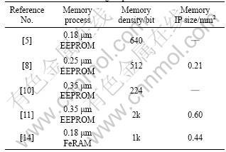
Table 1 shows the comparison of capacities and IP sizes on various EEPROMs for UHF RFID tag chip. EEPROM processes adopt a logic process instead of an embedded EEPROM process to reduce prices per wafer [15]. In this work, an EEPROM IP based on Tower’s c-flash cells was designed. The c-flash cells guarantees
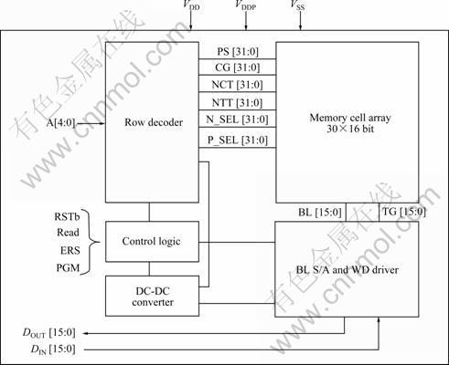
Fig.1 Block diagram of asynchronous 512-bit EEPROM
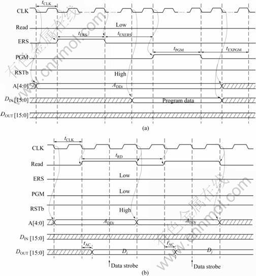
Fig.2 Timing diagrams of the EEPROM: In write mode (a); In read mode (b)
Table 1 Comparison of capacities and IP sizes on various EEPROMs for UHF RFID tag chip
1 000 erase-program cycles and data retention of 10 years. Fig.3 shows the circuit of Tower’s c-flash memory cell. The c-flash memory cell of the designed 512-bit EEPROM consists of a control capacitor (C1), a tunneling capacitor (C2), a read-out inverter (MP1 and MN1) and a CMOS transmission gate (MP2 and MN2). NMOS and PMOS transistors of 3.3 V are used. The phantom cell size is 21.35 ?m×68.69 ?m based on a 16-bit word.
Table 2 shows the bias voltages of a c-flash memory cell in different operation modes. In the erase mode, electrons of the floating gate are ejected by the Fowler-Nordheim (FN) tunneling with CG and TG applied with -4.75 V and 4.75 V, respectively. In the program mode, electrons of the floating gate are ejected by the FN tunneling with CG and TG applied with 4.75 V and -4.75 V, respectively. In the read mode, the erased cell outputs 0 V on the BL while the programmed cell outputs VDD.
Fig.4(a) shows a CG driving circuit supplying CG, power supply (PS), N_SEL and P_SEL with the bias voltages of Table 2 according to relative operation modes. Fig.4(b) shows a TG driving circuit supplying TG according to the operation modes and write data (WD). As shown in Fig.4, switching powers from VCG_HV, VCG_LV,
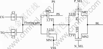
Fig.3 Circuit of Tower’s c-flash memory cell
Table 2 Bias voltages of c-flash memory cell at different node in different operation modes

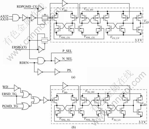
Fig.4 Driving circuits for VCG (a) and VTG (b)
VTG_HV, VTG_LV, VNNL_CG, and VNNL_TG switching circuits are supplied for the CG and TG driving circuits according to the operation modes shown in Table 2. The CG driving circuit in Fig.4(a) uses three stages of the voltage level translator circuit where it switches between VDD and VNNL_CG, between VCG_HV and VNNL_CG, and between VCG_HV and VCG_LV to have switching voltages under 4.75 V. Table 3 shows the output voltages of switching powers. From Table 3, it can be seen that switching voltages of each voltage level translator are all under 4.75 V according to the operation modes. Since the TG driving circuit in Fig.4(b) also uses three stages of the voltage level translator circuits switching between VDD and VNNL_TG, between VTG_HV and VNNL_TG, and between VCG_HV and VCG_LV, its switching voltages are all under 4.75 V.
Table 3 Output voltages of switching powers according to the operation modes
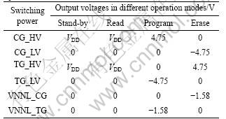
Fig.5 shows the switching power circuits for VCG_HV and VCG_LV, Fig.6 for VTG_HV and VTG_LV, and Fig.7 for VNNL_CG and VNNL_TG. VCG_LV in Fig.5 uses three stages of
voltage level translators switching between VDD and VNNL, between VSS (voltage of virtual ground) and VNNL, and between VSS and VNN in the write mode. Since the N-well voltage, body of MPCG-PMOS transistor of VCG_LV node, is designed to switch to 0 V in the erase mode, VCG_HV and VCG_LV circuits are designed to switch under 4.75 V. The circuit in Fig.6 is similar to that in Fig.5, and N-well voltage, body of MPTG, is designed to switch to 0 V in the program mode. In addition, VNNL_CG and VNNL_TG in Fig.7 are designed to those listed in Table 3 according to the operation modes.
The conventional EEPROM for a RFID tag chip uses a reference voltage generator to supply the reference voltage to a pumping voltage in the write mode [5]. In this case, power consumption will increase in the write mode since both the EEPROM and the analog block have their own reference voltage generators. Thus, the reference voltages VREF_VPP for VPP and VREF_VNN for VNN are used by dividing VDD supplied from the analog block in stead of removing the reference voltage generators to reduce a power consumption of EEPROM in the write mode in this work.
Fig.8 shows a positive voltage VPP (=4.75 V) generation circuit where high voltage is supplied in the write mode. The VPP generation circuit consists of a two-stage cross coupled charge pump, a control logic unit, a ring oscillator, and a level detector. VPP will go up by the positive pumping since the output signal of the VPP level detector, VPP_OSC_ENb, is low when VPP is lower than the target voltage. VPP is kept to the target voltage of 4.75 V since VPP_OSC_ENb is high and as a result, charge pumping stops from a negative feedback generated when
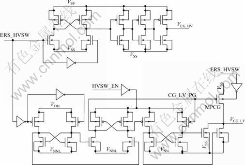
Fig.5 Switching power circuits for VCG_HV and VCG_LV
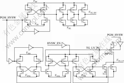
Fig.6 Switching power circuits for VTG_HV and VTG_LV

Fig.7 Switching power circuits for VNNL_CG (a) and VNNL_TG (b)
VPP is greater than the target voltage. The reference voltage, VREF_VPP (=0.678 5 V), of the level detector is generated by dividing VDD with a capacitive divider in Fig.9. It will be possible to make a low-power memory using the capacitive divider instead of a resistive divider since the capacitive divider removes the bias current in the write mode. Adding a delay chain to the positive pumping voltage detector to make a voltage division after discharging a PMOS switch (MP1), NMOS switches (MN1 and MN2), and every node of capacitors, VPP can be stable since it uses an exact reference voltage made by dividing the difference of voltage between VPP and VSS that is always 0 V by the PMOS switch and the NMOS switches although VPP is boosted from VDD. The charge pump in Fig.8 uses a cross-coupled type [15].
Fig.10 shows a VNN generation circuit for VNN (=-4.75 V) and VNNL (=VNN/2) by using six stages of charge pumps that are NMOS diode types. VNN is kept to -4.75 V by a negative feedback and VNNL supplies VNN/2 since it is the output voltage of the first stage charge pump. Fig.11 shows the proposed VNN voltage detector circuit using a capacitive divider.
Fig.12 shows the proposed VSS precharge circuit. The proposed VSS precharge circuit turns off MN3 and makes the voltage between the gate and the source of MN2 under 5.5 V simultaneously. This occurs since the node voltage of N2 is switched from VDD to 0 V by a capacitive coupling in entering the write mode. The

Fig.8 Block diagram of VPP generation circuit
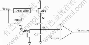
Fig.9 VPP voltage detector circuit
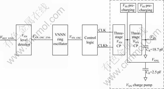
Fig.10 VNN generation circuit
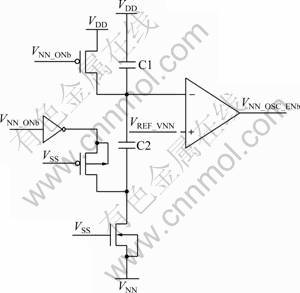
Fig.11 Proposed VNN voltage detector circuit
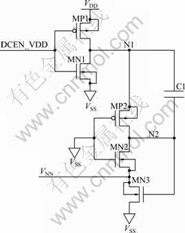
Fig.12 Proposed VSS precharge circuit
voltage between the source and the drain of MP2 is kept under 5.5 V by a capacitive coupling of C1 in exiting from the write mode.
When VPP powers up from VDDP (2 V supply voltage) to 4.75 V and VNN from 0 V to -4.75 V simultaneously in the write mode, a voltage drop of VDDP from the big power dissipation of the DC-DC converter causes a malfunction for the RFID tag chip. Thus, the sequential pumping scheme and a new ring oscillator with a dual oscillation period are proposed to reduce the power dissipation. Also, a stable supply of power generation for the RFID tag chip occurs when entering the write mode.
The sequential pumping means a scheme that first pumps VNN of -4.75 V and then pumps VPP of 4.75 V. Thus, the power dissipation is distributed by controlling the power-ups of VNN and VPP sequentially. In contrast, power dissipation required for a continuous charge pumping at power-up is greater than that required for an intermittent charge pumping in the steady state after power-up. Thus, a ring oscillator with a dual oscillation period is proposed such that it has a longer period in entering the write mode and a shorter period in the steady state. Fig.13 shows the proposed ring oscillator. The sequential pumping scheme and the ring oscillator with a dual oscillation period prevent VDDP from lowering by distributing the power dissipation like this during the power-up.
3 Simulation results
We designed a 512-bit EEPROM IP based on a 0.18 μm logic process. Fig.14 shows simulation results of cell bias voltages in the erase and program modes. It is confirmed that the results correspond to those in Table 2.
Fig.15 shows the timing diagram for the control signals in the read mode and important internal signals. If read signal enters in the read mode, a word of cells is first selected by PS, N_SEL, and P_SEL, and then CG switches from 0 V to VDD. Finally, BL voltage is precharged or discharged according to the written state of cell. A word of cells transfers to BL, and then a read-out word of BL is sensed and outputted to DOUT if SAENb signal is activated low. Under the slow simulation condition, the read access time is 195 ns.
Fig.16 shows simulation results with respect to sequential pumping of VPP and VNN in the write mode. From Fig.16, it can be seen that VPP is pumped to 4.75 V after VNN is pumped to -4.75 V.
Table 4 shows the simulation results for active currents and power dissipations where the cycle time in the read, program and erase modes is 12.58 μs, 1.2 ms and 1.2 ms, respectively. The power dissipation under the typical condition is 0.34 ?W in the read mode, 13.76 ?W in the program mode, and 13.66 ?W in the erase mode, respectively. In addition, Table 5 shows the comparison between power dissipations in the read and write mode of the proposed EEPROM and that of conventional ones.
The layout image of the designed 512-bit EEPROM IP using the 0.18 ?m logic process is shown in Fig.17 and its layout size is 373.96 ?m×434.04 ?m.
4 Conclusions
(1) To reduce a power consumption of EEPROM in
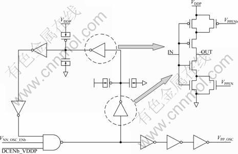
Fig.13 Proposed ring oscillator circuit with dual oscillation period
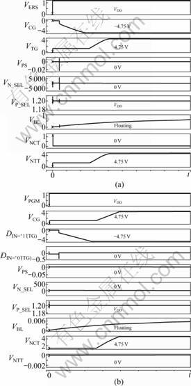
Fig.14 Simulation results of cell bias voltages (V): (a) In erase mode; (b) In program mode
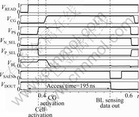
Fig.15 Simulation results with respect to critical path in read cycle (VDD=1.08 V, SS (NMOS: Slow, POMS: Slow) model, -40 ℃)
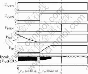
Fig.16 Simulation results with respect to sequential pumping of VNN and VPP in write mode (TT model, 25 ℃, VDD=1.2 V, VDDP=2 V)
Table 4 Active currents and power dissipations for different operation modes (VDD=1.2 V, VDDP=2 V, TT (NMOS: Typical, PMOS: Typical) model, 25 ℃)
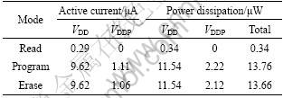
Table 5 Comparison between power dissipation of proposed EEPROM and that of conventional one
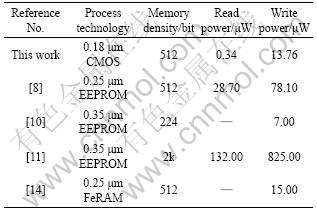
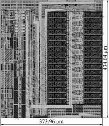
Fig.17 Layout image of designed 512-bit EEPROM IP
the write mode, the reference voltages VREF_VPP for VPP and VREF_VNN for VNN are used by dividing VDD supplied from the analog block in stead of removing the reference voltage generators. A voltage level detector using a capacitive divider is also proposed as a low-power DC-DC converter design technique. It is confirmed by the computer simulation that the power dissipations are 0.34 ?W in the read mode, 13.76 ?W in the program mode, and 13.66 ?W in the erase mode.
(2) Only logic process-based devices are used for this study. To secure reliability, voltages of devices of 3.3 V are kept under 5.5 V in the write mode. EEPROM core circuits, control gate (CG) and tunnel gate (TG) driving circuit are proposed; and DC-DC converters: Vpp (=4.75 V), VNN (-4.75 V), and VNNL (=VNN/2) generation circuit are also proposed.
(3) To generate a stable power supply voltage, charge pumps of VPP and VNN are turned on sequentially in entering the write mode. In addition, a ring oscillator with the dual oscillation period is proposed newly to reduce the inrush current of the power supply.
(4) The 512-bit EEPROM IP is designed with c-flash cells of Tower’s 0.18 ?m process. The layout area is 373.96 ?m×434.04 ?m.
References
[1] WEINSTEIN R. RFID: A technical overview and its application to the enterprise [J]. IT Professional, 2005, 7(3): 27-33.
[2] Yi W J. A low-power EEPROM design for UHF RFID tag chip [J]. Journal of Korea Institute of Maritime Information and Communication Sciences, 2006, 10(3): 486-495.
[3] AHMED A, KHALED S, MAGDI I. A compact low-power UHF RFID tag [J]. Microelectronics Journal, 2009, 40(11): 1-10.
[4] XI Jing-tian, YAN Na, CHE Wen-yi, XU Cong-hui, WANG Xiao, YANG Yu-qing, JIAN Hong-yan, MIN Hao. Low-cost low-power UHF RFID tag with on-chip antenna [J]. Journal of Semiconductors, 2009, 30(7): 1-6.
[5] PAN Li-yang, LUO Xian, YAN Ya-ru, MA Ji-rong, WU Dong, XU Jun. Pure logic CMOS based embedded non-volatile random access memory for low power RFID application [C]// Proceedings of Custom Integrated Circuits Conference. California: IEEE Press, 2008: 197-200.
[6] UDO K, MARTIN F. Fully integrated passive UHF RFID transponder IC with 16.7 μW minimum RF input power [J]. Journal of Solid-State Circuits, 2003, 38(10): 1602-1608.
[7] LEE J H, KIM J H, LIM G H, KIM T H, LEE J H, PARK K H, PARK M H, HA P B, KIM Y H. Low-power 512-bit EEPROM designed for UHF RFID tag chip [J]. ETRI Journal, 2008, 30(3): 347-354.
[8] BAEK S M, LEE J H, SONG S Y, KIM J H, PARK M H, HA P B, AND KIM Y H. A design on low-power and small-area EEPROM for UHF RFID tag chips [J]. Journal of Korea Institute of Maritime Information and Communication Sciences, 2007, 11(12): 2366-2373.
[9] BARNETT R E, LIU J. An EEPROM programming controller for passive UHF RFID transponders with gated clock regulation loop and current surge control [J]. Journal of Solid-State Circuit, 2008, 43(8): 1808-1815.
[10] LIU Dong-sheng, ZOU Xue-cheng, ZHANG Fan, DENG Min. Embedded EEPROM memory achieving lower power: New design of EEPROM memory for RFID tag IC [J]. IEEE Circuits and Devices Magazine, 2006, 22(6): 53-59.
[11] YARON G. A 16K E/SUP 2/PROM employing new array architecture and designed-In reliability features [J]. Journal of Solid-State Circuit, 1982, 17(5): 833-840.
[12] USAMI M, SATO A, SAMESHIMA K, WATANANBE K, YOSHIGI H, IMURA R. Power LSI: An ultra small RF identification chip for individual recognition applications [C]// Solid-State Circuit Conference. Lodon: IEEE Press, 2003: 398-501.
[13] KANG H B, HONG S K, SONG Y W, SUNG M Y, CHOI B G, CHUNG J Y, LEE J W. High security FeRAM-based EPC C1G2 UHF (860 MHz-960 MHz) passive RFID tag chip [J]. ETRI Journal, 2008, 30(6): 826-832.
[14] ROIZIN Y. C-flash: An ultra-low power single poly logic NVM [C]// International Conference on Memory Technology and Design. Opio: Tower Semicond. Ltd., 2008: 90-92.
[15] LIM G H, SONG S Y, PARK J H, LI LONGZHEN, LEE C H, LEE T Y, CHO G S, PARK M H, HA P B, KIM Y H. Charge pump design for TFT-LCD driver IC using stack-MIM capacitor [J]. IEICE Transactions on Electronics, 2008, E91-C(6): 928-935.
(Edited by LIU Hua-sen)
Foundation item: Project supported by the Second Stage of Brain Korea 21
Received date: 2010-01-12; Accepted date: 2010-03-30
Corresponding author: KIM Y H; Tel: +86-55-2851023; E-mail: youngkim@changwon.ac.kr