文章编号:1004-0609(2008)01-0048-06
退火处理对ITO和ITO?Zr薄膜性能的影响
张 波1,董显平1,徐晓峰2,赵 培3,吴建生1
(1. 上海交通大学 材料科学与工程学院 教育部高温材料及测试重点实验室,上海 200240;
2. 东华大学 理学院,上海 200051;
3. 中国科学院 上海技术物理研究所,上海 200083)
摘 要:利用磁控溅射在室温条件下沉积ITO薄膜和ITO?Zr薄膜,对比研究在空气中退火处理对ITO和ITO?Zr薄膜性能的影响。结果表明,Zr的掺杂促进了(400)晶面的取向,随着退火温度的升高,薄膜表面颗粒增大,表面粗糙度有所降低。室温下Zr的掺杂显著改善了薄膜的光电性能,随着退火温度的升高,ITO和ITO?Zr薄膜的方阻都表现为先降后升的趋势,ITO?Zr薄膜在较低的退火温度下可见光透过率就可达到80%以上,直接跃迁模型确定的光学禁带宽度Eg呈现了先升后降的变化。ITO?Zr薄膜比ITO薄膜显示了更高的效益指数,揭示了ITO?Zr薄膜具有更好的光电性能。
关键词:ITO薄膜;磁控溅射;退火处理;光电性能
中图分类号:O 484.4 文献标识码:A
Effect of annealing treatment on properties of
ITO and ITO?Zr thin films
ZHANG Bo1, DONG Xian-ping1, XU Xiao-feng2, ZHAO Pei3, WU Jian-sheng1
(1. Key Laboratory for High Temperature Materials and Tests of Ministry of Education,
School of Materials Science and Engineering, Shanghai Jiao Tong University, Shanghai 200240, China;
2. College of Science, Donghua University, Shanghai 200051, China;
3. Shanghai Institute of Technical Physics, Chinese Academy of Science, Shanghai 200083, China)
Abstract: ITO and ITO?Zr thin films were deposited at room temperature by magnetron sputtering. Properties of ITO and ITO?Zr thin films by air-annealing treatment were contrastively studied. The results show that Zr-doping promotes the orientation of (400) plane. With the increase of annealing temperature, the grain size increases and the surface roughness decreases. Zr-doping remarkably improves the optical-electronic characteristics of the films deposited at room temperature. With the increase of annealing temperature, the sheet resistances of ITO and ITO?Zr thin films show the trend that first drops and then rises. ITO?Zr thin films have high optical transmittance of above 80% at lower annealing temperature. The direct transition model was established and band gap energy Eg was obtained, which show the change that Eg increases and follows by a sudden drop. ITO?Zr thin films reveal higher figure of merit than ITO thin films, which reveals that ITO?Zr thin films have better optical-electrical properties.
Key words: ITO thin films; magnetron sputtering; annealing treatment; optical-electrical properties
掺锡氧化铟(Indium Tin Oxide,简称ITO)薄膜是一种重掺杂、高简并的n型半导体,由于其具有优异的透明性和导电性,被广泛应用于电子工业、屏蔽防护和太阳能等领域[1?2]。随着应用领域的不断拓展,三元ITO薄膜已无法满足各种性能的要求,目前ITO基多元体系得到了一定的发展[3?4],HSU等[5]利用双靶共溅射在ITO薄膜的表面层进行了掺Ni处理,Ni的掺入在促进ITO薄膜晶化的同时,降低了表面粗糙度,提高 了表面功函数,但掺Ni却没有提高薄膜的光电性。SUZUKI等[6]利用质量比m(In2O3)? m(SnO2)? m(V2O5)= 94.05?4.95?1的靶材进行了ITO薄膜的V掺杂,V的掺入提高了载流子浓度,但降低了迁移率。不同元素的掺杂往往只是为了提高ITO薄膜的特定性能,因此在保持或提高ITO薄膜光电性能的前提下,同时改善其它物化性能是掺杂ITO薄膜的研究重点。
磁控溅射常用于溅射各类薄膜,对于ITO薄膜来说,可以通过双靶共溅射进行高价金属元素(如Zr)的掺杂,通过施主原子取代晶格位置产生多余的自由电子,以得到性能更优异的多元复合透明导电氧化物(TCO)薄膜。多元体系ITO?Zr薄膜既可以保持传统ITO薄膜的性能,又可以通过改变掺杂组分而调整薄膜的光电性能、物化性质和表面能等,从而可以提高ITO薄膜的各项性能指标。
本文作者利用磁控溅射法在室温条件下制备ITO和ITO?Zr薄膜,对比研究退火处理对ITO 和ITO?Zr薄膜性能的影响,利用各种测试手段对退火后的晶体结构、表面形貌以及光电性能等进行表征和对比。
1 实验
采用JPGF?400B?G型磁控溅射仪在玻璃衬底上制备了ITO薄膜和ITO?Zr薄膜,ITO和ITO?Zr薄膜的制备工艺保持一致,只是在制备ITO?Zr薄膜时引入了射频溅射金属Zr靶,ITO?Zr薄膜是以ITO靶(直流45 W)和金属Zr靶(射频10 W)双靶共溅射制备得到。ITO靶(In2O3质量分数90%,SnO2质量分数10%)和Zr靶的纯度都为99.99%,靶直径为62 mm,基片与靶的距离为65 cm,本底真空度为10?4 Pa,氧流量为0.3 cm3/min。通过控制Ar气流量使工作气压保持在0.5 Pa,在镀膜前对靶材表面进行3 min的预溅射,溅射镀膜时间都为30 min。Zr的掺入未引起薄膜厚度的明显变化,薄膜厚度大约都为240 nm。在优化工艺条件下,ITO和ITO?Zr薄膜中金属摩尔比分别为:n(In)?n(Sn)=9?1;n(In)?n(Sn)?n(Zr)=9?1?0.2。样品在退火炉(空气气氛)各退火温度下处理时间都为35 min。
实验采用Dektak 6M台阶仪测定薄膜的厚度,采用SDY?5四探针测试薄膜的方阻,采用爱建公司AJ?Ⅲ型AFM进行观察薄膜的形貌,采用D/max 2550VX射线衍射仪对薄膜样品进行物相分析及晶粒测定,采用Lamda950型UV?VIS?NIR分光光度计测量薄膜的透射光谱。
2 结果与讨论
2.1 退火处理对薄膜晶体结构和表面形貌的影响
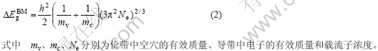
图1所示分别为ITO 和ITO?Zr薄膜在不同退火温度下的XRD谱。可以发现,随着退火温度的上升,(222)和(400)晶面的衍射峰强度显著增强,(211)、(440)和(622)等晶面取向也变得清晰起来,这说明退火处理提高了薄膜的晶化程度,促使了薄膜由微晶向多晶体的转变。图2中I(222)/I(400)强度比的变化显示了(222)晶面取向占据了主导地位,这是因为退火处理是在空气中进行,富氧状态促进了(222)晶面的取向,而且随着退火温度的升高,I(222)/I(400)强度比略有升高。薄膜生长是一种氧化性与脱氧性竞争的过程,而这种竞争对(222)和(400)择优取向的变化有着深刻的影响[7]。Zr的掺入在促进晶体生长的同时会促使(400)晶面取向的加强。
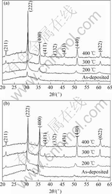
图1 ITO 和 ITO?Zr薄膜在不同退火温度下的XRD谱
Fig.1 XRD patterns of ITO and ITO?Zr thin films at different annealing temperatures: (a) ITO thin films; (b) ITO?Zr thin films
由布拉格和晶面间距公式可算出晶面间距和晶格常数,可以发现,随着退火温度的升高,薄膜晶格常数相应变小,其原因可能是溅射沉积的薄膜中存在压应力,退火处理使得应力得以释放。图1中XRD(222)峰位的迁移也证实了这一点,同时也发现,由于Zr的掺入,ITO?Zr薄膜比ITO薄膜具有更大的晶格常数(见图2)。可由Scherrer公式:

图2所示为ITO 和 ITO?Zr薄膜在不同退火温度下的晶粒尺寸和半高宽(FWHM)的变化。由图可见,随着退火温度的升高,半高宽逐渐变窄,晶粒有所长大;当退火温度高于 300 ℃时,ITO?Zr薄膜晶粒大小已趋于稳定,这表明晶化程度已比较充分,ITO?Zr薄膜比ITO膜薄具有更大的晶粒尺寸;在相对较低的退火温度下,ITO?Zr薄膜的晶化程度比ITO膜薄高,Zr的掺入促进了薄膜的晶化。

图2 ITO 和 ITO?Zr 薄膜在不同退火温度下的I(222)/ I(400)强度比和晶格常数、晶粒尺寸和半高宽
Fig.2 Variations of I(222)/I(400) ratio, lattice parameter, grain size and FWHM of ITO and ITO?Zr thin films as function of annealing temperature
图3所示为ITO 和ITO?Zr薄膜在室温制备和 400 ℃退火温度下的AFM像。可以发现,经过退火处理,薄膜的表面颗粒有了显著的长大[8]。当薄膜在低温生长时,由于生长过程中能量的缺失以及能量粒子对膜表面的轰击,使得表面存在一些异常生长的颗粒。通过AFM剖面线性扫描可知,ITO薄膜的均方根粗糙度Rrms由1.03 nm降为0.79 nm,ITO?Zr薄膜的Rrms也由1.01 nm降为0.76 nm。经过退火处理后的ITO?Zr薄膜具有相对较小的表面粗糙度,而薄膜的表面形貌与表面粗糙度对于薄膜的表面能和光电性能都有着直接的影响。

图3 ITO和ITO?Zr薄膜在室温制备和400 ℃退火温度下的AFM像(1 000 nm×1 000 nm)
Fig.3 AFM images of ITO and ITO?Zr thin films at as-deposited and annealing at 400 ℃: (a), (b) ITO thin films; (c), (d) ITO?Zr thin films
2.2 退火处理对薄膜光电性能的影响
图4所示为ITO 和ITO?Zr薄膜在不同退火温度下方阻的变化,图5所示分别为ITO 和ITO?Zr薄膜在不同退火温度下的透射光谱(包含玻璃基底)。可以发现,随着退火温度的不断提高,ITO 和ITO?Zr薄膜的电阻都呈现了先降后升的趋势,而二者在可见光区的透过率都有所上升。
在一定处理温度范围内,薄膜的光电性能有了显著的改善,这是由于随着退火温度的提高,薄膜的结晶性、晶粒大小、缺陷和晶界等均发生了明显变化。在ITO薄膜中,Sn一般以SnO(二价)或SnO2(四价)的形式存在,Sn2+对In3+是一种p型掺杂,这会降低ITO薄膜的载流子浓度而提高膜的方阻,此外,SnO呈暗褐色而对可见光的透过率较差。经过退火处理,一方面能促使SnO向SnO2转变,促进晶格生长;另一方面能促使薄膜中多余的氧脱附,从而达到降低薄膜方阻、提高薄膜可见光透过率的目的。随着温度的进一步升高,ITO 和ITO?Zr薄膜的方阻都呈现了上升的趋势,这可能是由于:一方面,过高的退火温度促使晶格振动加剧,形成一些晶格缺陷使晶格变得不完整,而这些缺陷又会成为散射中心,使方阻有所上升;另一方面,在高温环境条件下,玻璃基底中的碱性金属离子极易迁移到薄膜中,使薄膜的性能变坏[9]。在200 ℃至 400 ℃的退火温度区间里,ITO?Zr薄膜的方阻比ITO薄膜的略大,这可能是由于Zr原子对氧具有一定的亲和力作用,一定量的氧进入薄膜中相对减少了氧空位的浓度[10]。对于ITO薄膜来说,退火温度的进一步升高使得方阻上升较明显,而ITO?Zr薄膜的方阻变化不大,这从侧面揭示了ITO?Zr薄膜具有更好的热稳定性。

图4 ITO 和ITO?Zr薄膜在不同退火温度下的方阻
Fig.4 Variations of sheet resistance of ITO and ITO?Zr thin films as function of annealing temperature
图5所示的透射光谱表明,随着退火温度的上升,可见光区的透过率相应有所提高。这是由于薄膜结晶化程度以及组织均匀性得到了提高,而缺陷浓度有所降低,这些都减少了对光的散射损失。通过对比发现,Zr的掺入明显提高了薄膜在可见光区的透过率,改善了薄膜的光学性能。对于ITO薄膜来说,当退火温度小于300 ℃时,其可见光的透过率不到60%,而ITO?Zr薄膜在较低的退火温度下透过率就可达到80%以上。近红外区域的透过率与载流子密度密切相 关[11],近红外区透过率的变化趋势体现了自由载流子对长波的反射作用。

图5 ITO和ITO?Zr薄膜在不同退火温度下的透射光谱
Fig.5 Optical transmittance spectra of ITO and ITO?Zr thin films at different annealing temperatures: (a) ITO thin films; (b) ITO?Zr thin films
薄膜的紫外吸收界限随着退火温度的升高开始向紫外UV 区域移动,即薄膜发生了蓝移现象,这主要是由于“Burstin?Moss”效应(“B?M”效应)[12]引起的。对于未掺杂的In2O3材料,费米能级EF位于导带和价带中间,随着低密度施主的引入,在导带底下面会形成了n型施主杂质能级,费米能级EF位于导带底和施主能级之间。由于掺杂量的增加导致了施主态密度的提高,又由于ITO薄膜是一种重掺杂,其结果导致了导带中低能态被电子所填充,较高电子浓度的电子占据了导带的底端,使得光学能隙产生了宽化。
ITO薄膜在紫外区的吸收是由薄膜中的载流子浓度Ne所决定的,由“B?M”效应引起的宽化能带可以表示为
式(2)表明薄膜中载流子浓度的增大将导致薄膜光学禁带的宽化[13]。光子在紫外区的吸收与TCO的禁带能隙密切相关。对于宽禁带直接跃迁半导体材料有:αE=A(E?Eg)1/2, 吸收系数(α)近似等于:α=ln(1/T)/d,其中Eg为直接光学禁带宽度,E为光子流量,d为薄膜厚度,T为透过率。作出(αE)2与光子能量(E)的关系图,对线性部分进行拟合外推,横坐标的截距就是禁带宽度Eg的值[14]。如图6所示,对比ITO和ITO?Zr薄膜在不同退火温度下禁带宽度的变化可知,通过直接跃迁模型和线性外推确定的光学禁带宽度Eg呈现了先升后降的变化,在一定退火温度范围内,ITO?Zr比ITO薄膜具有更窄的光学禁带。

图6 ITO和ITO?Zr薄膜在不同退火温度下的光学禁带宽度
Fig.6 Variations of optical band gap of ITO and ITO?Zr thin films as function of annealing temperature
2.3 ITO和ITO?Zr薄膜综合性能的对比
一般以效益指数φTC(φTC = Ta10/Rsq,其中Ta为可见光区的平均透过率,Rsq为方阻)作为评价TCO薄膜光电性能的指标[15?16]。图7所示为 ITO和ITO?Zr薄膜在不同退火温度下效益指数的变化。由图可见,随着退火温度的上升,ITO和ITO?Zr薄膜的效益指数 φTC都呈现了上升的趋势,ITO薄膜由0.003×10?3 Ω?1上升到了4.53×10?3 Ω?1,ITO?Zr薄膜也由0.15×10?3 Ω?1上升到了5.43×10?3 Ω?1,ITO?Zr薄膜比ITO薄膜具有更高的效益指数,揭示了ITO?Zr薄膜具有更好的光电性能。相关性能测试表明,Zr的掺入提高了ITO薄膜的表面能(水接触角明显下降),提高了热稳定性和化学稳定性,同时降低了由于相转变而导致光电性能的变化,可以认为多元复合体系TCO薄膜(ITO?Zr薄膜)比传统的ITO薄膜具有更好的综合性能。

图7 ITO和ITO?Zr薄膜在不同退火温度下的效益指数
Fig.7 Figure of merit  of ITO and ITO?Zr thin films as function of annealing temperature
3 结论
1) 对比讨论了ITO 和ITO?Zr薄膜在不同退火温度下各种性能的变化。随着退火温度的升高,晶格常数和表面粗糙度都有所下降。但Zr的掺入促进了(400)晶面的取向,ITO?Zr薄膜比ITO薄膜具有更大的晶格常数和颗粒尺寸以及较低的表面粗糙度。
2) 室温下Zr的掺杂显著改善了薄膜的光电性能,随着退火温度的升高,ITO和ITO?Zr薄膜的方阻都显现出先下降后上升的趋势,较低退火温度的条件下,ITO?Zr薄膜的可见光透过率就可达到80%以上,薄膜的光学禁带宽度Eg都呈现了先升后降的变化,一定的退火温度范围内,ITO?Zr比ITO薄膜具有更窄的光学禁带。
3) ITO?Zr薄膜比ITO薄膜具有更高的效益指数,揭示了ITO?Zr薄膜具有更好的光电性能,同时,相关测试表明ITO?Zr薄膜比ITO薄膜具有更好的综合性能。
REFERENCES
[1] BESBES S, OUADA H B, DAVENAS J, PONSONNET L, JAFFREZIC N, ALCOUFFE P. Effect of surface treatment and functionalization on the ITO properties for OLEDs[J]. Materials Science and engineering C, 2006, 26: 505?510.
[2] 姜文龙, 段 羽, 刘式墉. 无氧溅射方法制备OLED的ITO透明电极[J]. 光电子?激光, 2007, 18(2): 129?131.
JIANG Wen-long, DUAN Yu, LIU Shi-yong. Fabrication of OLED ITO transparent electrode with oxygen-free sputtering method[J]. Journal of Optoelectronics Laser, 2007, 18(2): 129?131.
[3] MIYATA T. Transparent conducting zinc-co-doped ITO films prepared by magnetron sputtering[J]. Thin Solid Films, 2000, 373: 189?194.
[4] NAKASA A, ADACHI M, USAMI H, SUZUKI E, TANIGUCHI Y. Fabrication of nickel oxide and Ni-doped indium tin oxide thin films using pyrosol process[J]. Thin Solid Films, 2006, 498: 240?243.
[5] HSU C M, LEE J W, MEEN T H, WU W T. Preparation and characterization of Ni-indium tin oxide cosputtered thin films for organic light-emitting diode application[J]. Thin Solid Films, 2005, 474: 19?24.
[6] SUZUKI M, MAEDA Y, MURAOKA M, HIGUCHI S, SAWADA Y. ITO films sputter-deposited using an ITO target sintered with vanadium oxide additive[J]. Mater Sci Eng B, 1998, 54: 43?45.
[7] QUAAS M, STEFFEN H, HIPPLER R, WULFF H. Investigation of diffusion and crystallization processes in thin ITO films by temperature and time resolved grazing incidence X-ray diffractometry[J]. Surface Science, 2003, 540: 337?342.
[8] 赵透玲, 任丙彦, 赵 龙, 王文静. 射频磁控溅射ITO薄膜中沉积温度对膜特性影响[J]. 光电子?激光, 2005, 16(12): 1429?1432.
ZHAO Xiu-ling, REN Bing-yan, ZHAO Long, Wang Wen-jing. Effect of deposition temperature on ITO thin films prepared by RF magnetron sputtering[J]. Journal of Optoelectronics Laser, 2005, 16(12): 1429?1432.
[9] BISWAS P K, DE A, PRAMANIK N C, CHAKRABORTY P K, ORTNER K, HOCK V, KORDER S. Effect of tin on IR reflectivity, thermal emissivity, Hall mobility and plasma wavelength of sol-gel indium tin oxide films on glass[J]. Material Letters, 2003, 57: 2326?2332.
[10] QADRI S B , KIM H, KHAN H R, PIQUE A, HORWITZ J S, CHRISEY D, KIM W J. Transparent conducting films of In2O3-ZrO2,SnO2-ZrO2 and ZnO-ZrO2[J]. Thin Solid Films, 2000, 377: 750?754.
[11] BENDER M, SEELIG W, DAUBE C, FRANKENBERGER H, OCKER B, STOLLENWERK J. Dependence of oxygen flow on optical and electrical properties of DC-magnetron sputtered ITO films[J]. Thin Solid Films, 1998, 326: 72?77.
[12] HAMBERG I, GRANQVIST C G. Theoretical model for the optical properties of In2O3: Sn films in the 0.3?50 μm range[J]. Solar Energy Materials, 1986, 14: 241?256.
[13] 李世涛, 乔学亮, 陈建国. 射频磁控溅射沉积ITO薄膜性能及导电机理[J]. 中国有色金属学报, 2006, 16(4): 688?693.
LI Shi-tao, QIAO Xue-liang, CHEN Jian-guo. Properties and conductivity mechanism of ITO films prepared by r. f. magnetron sputtering[J]. The Chinese Journal of Nonferrous Metals, 2006, 16(4): 688?693.
[14] GUILLEN C, HERRERO J. Influence of oxygen in the deposition and annealing atmosphere on the characteristics of ITO thin films prepared by sputtering at room temperature[J]. Vacuum, 2006, 80: 615?620.
[15] NISHA M, ANUSHA S, ANTONY A, MANOJ R, JAYARAJ M K. Effect of substrate temperature on the growth of ITO thin films[J]. Applied Surface Science, 2005, 252: 1430?1435.
[16] HAMID R F, MOHSEN G, ALI H, HADI S. The effect of annealing on structure, electrical and optical properties of nanostructured ITO films prepared by e-beam evaporation[J]. Materials Research Bulletin, 2007, 42: 487?496.
基金项目:上海应用材料基金资助项目(0525)
收稿日期:2007-05-08;修订日期:2007-09-20
通讯作者:张 波,博士研究生;电话:021-34203316;E-mail: glass114@163.com
(编辑 何学锋)

