
Improvement of epitaxy and crystallinity in YBa2Cu3Oy thin films grown on silicon with double buffer of ECO/YSZ
GAO Ju (�� ��)1, YANG Jian (�� ��)2
1. Department of Physics, University of Hong Kong, Pokfulam Road 100871, Hong Kong, China;
2. Beijing General Research Institute for Nonferrous Metals, Beijing 100088, China
Received 10 April 2006; accepted 25 April 2006
Abstract: A novel double buffer of Eu2CuO4 (ECO)/YSZ (yttrium-stabilized zirconia) was developed for growing YBa2Cu3Oy (YBCO) thin films on Si substrates. In these films, the severe reaction between Si and YBCO is blocked by the first YSZ layer, whereas, the degradation of crystallinity and superconductivity in the grown YBCO is greatly improved by the second ECO layer. Such an ECO material possesses a very stable 214-T�� structure and excellent compatibilities with YBCO and YSZ. The result shows that the epitaxy and crystallinity of YBCO deposited on Si could be considerably enhanced by using the ECO/YSZ double buffer. The grown films are characterized by high-resolution X-ray diffraction, grazing incidence X-ray reflection, and transmission electron microscopy (TEM), respectively. It is found that well defined interfaces are formed at YBCO/ECO/YSZ boundaries. No immediate layer could be seen. The defect density in all grown layers is kept at a lower level. The YBCO film surface turns out to be very smooth. These films have full superconducting transitions above 88 K and high current carrying capacity at 77 K. The successful growth of highly epitaxial YBCO thin films on silicon with ECO/YSZ buffer, demonstrate the advantages of such a double buffer structure.
Key words: YBa2O3Oy; High Tc superconductor; thin film; buffer material; microstructure
1 Introduction
Silicon is extensively used as substrates in semiconductor and electronic industry. Since the discovery of perovskite superconductors(HTSC), lots of efforts have been made to grow these oxides on silicon for their potential in various applications like superconductor/semiconductor hybrid devices and microelectronic circuits. However, attempts to grow HTSC thin films directly on Si were unsuccessful due to the severe reaction between Si and the grown films, which leads to a serious degradation of superconductivity and crystallinility in the grown films[1]. Thus the technique using a buffer layer is widely applied. Various materials such as yttrium stabilized ZrO2 (YSZ) [2], CeO2[3], SrTiO3 (STO)[4], MgO[5], PrBa2Cu3Oy[6], and SrBi2Ta2O3, are employed as the buffer material to block the interaction between HTSC film and Si substrate. Among various buffer materials, YSZ has been proved to most effectively block the diffusion of Si into YBa2Cu3Oy (YBCO). But the crystallinity and surface morphology of the grown YBCO films on YSZ buffered Si are rather poor due to the large lattice mismatch. An intermediate layer is frequently observed at the interface between YBCO and YSZ. It is mainly formed as BaZrO3 phase due to the diffusion of Ba into YSZ. The loss of Ba in the YBCO film leads to imperfection and discontinuities in the initially grown YBCO film[7]. In addition, the initial growth of YBCO films on YSZ showed significant island formation as revealed by transmission electron microscopy (TEM) and in-situ resistance measurement[8].
In our previous studies, 214T�� Eu2CuO4 (ECO) has been successfully used as a buffer for making ultra-thin films of YBCO on YSZ[9, 10]. Such an ECO material with a 214-T�� structure is very stable in crystal structure with no structural transition in a wide temperature range. It has excellent structural and chemical compatibilities with YBCO and YSZ. The in-plane lattice parameter a of ECO is about 0.389 nm and just lies between those of YBCO and YSZ. The lattice mismatch between ECO and YBCO is the smallest among all the known buffermaterials. ECO usually behaves like a semiconductor with high value of resistivity at low temperature. It is chemically compatible with YBCO and YSZ. No intermediate layer is formed at the interface between ECO and YSZ. Since ECO is also a high-Tc superconductor with a Tc of about 90 K, the diffusion of Eu into YBCO, if any, will not degrade the superconductivity of the grown films. Its very smooth surface would also benefit the further growth of YBCO films. We found that, by using the 214T buffer layer, the growth of YBCO thin films on YSZ can change from island growth mode to the layer-by-layer one[8].
Here we report a novel double buffer of ECO/YSZ for growing highly epitaxial YBCO films on Si wafer. By using such a double ECO/YSZ buffer, the epitaxy and crystallinity of the YBCO films grown on Si are remarkably improved. The grown films were characterized by X-ray diffraction(XRD) and grazing incidence reflection, rocking curve, scanning electron microscopy(SEM), and cross sectional TEM.
2 Experimental
Our films were deposited on Si (100) single crystal substrates by pulse laser deposition (PLD)[11]. The background vacuum is below 3��10-4 Pa and the deposition pressure is between 0.5 and 5.0��102 Pa. The deposition gas was a mixture of argon and oxygen (p(Ar)/p(O2) =3-4). An excimer laser with wavelength of 308 nm was used with the laser pulse energy of about 300 mJ and repetition rate of 5 Hz, respectively. The laser beam was focused by a lens onto the target at a density of about 4 J/cm2. The Si substrate was stuck on the heater by silver paste. The substrate temperature was 730-780 ��, which was measured by a k-type thermocouple inserted into the stainless substrate heater. The thickness of the film was measured by a Dektak3ST surface step profiler. The X-ray diffraction (XRD) was performed on the Siemens D5000 X-ray diffractometer with CuKa radiation (l=0.154 05 nm). The crystallinity of YBCO, ECO, and YSZ films was examined by measuring their rocking curves of (005) and (006) diffraction peaks respectively. High-resolution X-ray diffraction, X-ray small angle reflection, and X-ray reciprocal space mapping were performed on a high-resolution X-ray diffractometer (Bruker D8 Advance) at room temperature with CuK��1 radiation. The surface of the grown films was characterized by a Dektak3ST surface step profiler and a Cambridge 440 scanning electron microscope (SEM). The superconductivity was measured by a standard DC four-probe method using a closed-cycled cryostat.
3 Results and discussion
The phase structure formed in grown films was examined by XRD. The obtained diffraction spectra always reveal a coherent orientation of YBCO, ECO, and YSZ layers with the c-axis normal to the substrate surface. Typical XRD pattern for these films are shown in Fig.1. Only (00l) peaks for grown layers could be seen in XRD pattern. No reflections due to random crystallographic orientation or secondary phases appeared. To evaluate the quality of the epitaxy, rocking scans of (006) peak for YBCO film and (004) peak for ECO and YSZ buffer layers were performed (Fig.1). The rocking curves indicate very small values of the full width at half maximum (FWHM), 0.13? for YBCO, 0.12? for ECO and 0.10? for YSZ, respectively. For comparison, the FWHM value for the YBCO thin films grown on YSZ buffered Si substrate without ECO layer is about 0.26?. Small values of FWHM imply an excellent crystallinity of the grown YBCO films with the ECO/YSZ double buffer on silicon.
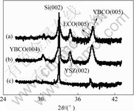
Fig.1 XRD patterns of different samples: (a) YBCO/Si; (b) YBCO/YXZ/Si; (c) YBCO/ECO/YSZ/Si
To determine the in-plane orientations of our films, f-scan measurements were carried out. The f-scans of the YBCO film and buffer layers showed single in-plane orientation with four-fold symmetry, demonstrating the achievement of heteroepitaxial growth. It is known that the growth of YBCO on YSZ have two different in-plane orientations due to the large lattice mismatching [8]. However, by adding the ECO buffer layer, we obtained single in-plane orientation in our YBCO films. The epitaxial orientation is c-axis perpendicular to the Si surface and the in-plane epitaxy is YBCO[100]//
ECO[100]//YSZ[110].
To clarify the interface microstructures of these films, high-resolution X-ray diffraction, X-ray small angle reflection, and X-ray reciprocal space map were performed on several samples. The X-ray small angle reflection is sensitive to the electron density and interfacial roughness of the each layer in a multilayer structure. Thus it can provide a powerful and non-destructive tool to investigate microstructures of thin films. The information of the multilayer structure such as the thickness and the interface roughness can be obtained by fitting the experimental data using a certain structural refinement model[8]. X-ray reflectivity profiles of our samples are shown in Fig.2. For the sample YBCO/Si, a transition layer of 5 nm was found between the YBCO and Si. This might be caused by a slight change of the chemical compositions at the vicinity of the YBCO/Si interface due to the severe lattice mismatch and strong diffusion between the film and substrate[1]. For the sample YBCO/YSZ/Si, an intermediate layer of BaZrO3 with a thickness of about 2 nm was formed at the YBCO/YSZ interface according to the theoretical simulation. It indicates that a chemical reaction at the YBCO/YSZ interface takes place and the Ba atoms diffuse into the YSZ layer. Such a BaZrO3 interlayer would result in the imperfection and degradation in the crystallinity and superconductivity in the YBCO film. Whereas, there is no intermediate layer at the interface of ECO/YSZ for the sample YBCO/ECO/YSZ/Si. Due to the existent of ECO, the chemical reaction between YBCO and YSZ is fully prevented. In other words, the epitaxy of the YBCO film deposited on Si is considerably enhanced by using an ECO/YSZ buffer.
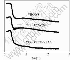
Fig.2 X-ray reflectivity profiles of different samples
The X-ray reciprocal space mapping of our samples provide further information about the misorientation, lattice mismatch and mosaic structure between the epilayers and substrate[12]. The results showed that strong mosaic structures exist in YBCO and YSZ layers, which are reconstructed from the Si substrate. From the reciprocal space map of the X-ray scattering, it is found that the quality of YBCO for the sample YBCO/ECO/YSZ/Si is significantly better than that for the sample YBCO/YSZ/Si, which well agreed with the foregoing results of the X-ray high-resolution diffraction and X-ray reflection measurements. The YSZ material is known having the least diffusion with YBCO layer thus it can effectively block the interaction between silicon and YBCO. However, the larger lattice constant
(a =0.514 nm) of the cubic YSZ leads to a remarkable lattice mismatch with YBCO (a =0.382 nm, b =0.389 nm and c=1.167 nm), approximately 4.5%-6.2%. If the YBCO is directly deposited on the YSZ buffer layer, there will be different orientations in the a-b plane even though the initial growing stage of the YBCO film could be island-like[8, 13]. The ECO buffer material possesses a stable tetragonal structure with a=0.390 nm and c=1.193 nm, matching well with that of YBCO. Therefore, the incompatibility between YSZ and YBCO would be reduced by adding an ECO interlayer. In this case, most mismatch stress would be located in the ECO sub-layer rather than in the YBCO layer, demonstrating advantages of an YSZ/ECO buffer.
Cross sectional TEM was used to study the interfaces between layers. A TEM image of an YBCO/ECO/YSZ/Si multilayer is shown in Fig.3. Well defined YBCO/ECO, ECO/YSZ, and YSZ/Si interfaces are evidences of the highly epitaxial growth. All layers are rather uniform and single crystal like. Moreover, the strain effects due to lattice mismatch are not likely appear as the TEM image shows sharp contrast for each layer. The high resolution TEM image demonstrates a high epitaxy of YBCO obtained on ECO/YSZ double buffered Si substrates. The TEM image also revealed that an amorphous layer of approximately 5 nm, probably in the form of SiO2, was formed between YSZ and Si. Such an oxide intermediate layer was found on all samples for TEM study. It is known as a native silicon oxide layer. Since the epitaxy of ECO layer is still remain, this oxide intermediate layer should be formed after epitaxy has been established through oxygen diffusion from YSZ into Si. On the other hand, the interface between YSZ and ECO is very clear. No intermediate layer, frequently observed at the YBCO/YSZ boundary, could be found. The formation of the BaZrO3 interlayer is fully prevented by adding the ECO second buffer.
Using such a double buffer of ECO/YSZ, full superconducting transitions with Tc,zero��90 K were obtained readily. The current carrying capacity at 77 K was about 5-8��105 A/cm2. Such a value of current density is reasonable for YBCO films grown on Si. Clearly, comparing with YBCO films on Si substrate with single YSZ buffer, the superconducting properties in these YBCO films grown on buffered Si substrates are much better and stable.
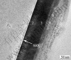
Fig.3 TEM image of cross section of YBCO/ECO/YSZ/Si thin film: 1 Si; 2 YSZ; 3 ECO; 4 YBCO
It is worthy to point out that the ECO buffer can enforce a very good surface morphology. Different from films of 1-2-3 compounds, films with the 214-T�� structure always reveal a very smooth and stable surface. The surface morphology and average roughness of our samples were characterized by using SEM, AFM, and surface profiler, respectively. The films grown on the ECO/YSZ buffered Si are very flat and smooth over a large area. No observable particles and surface structures are visible. The root mean square roughness of the film surface was evaluated with a large scanning length of 2 mm. For comparing, the samples were etched away using acid and the same scanning procedure was performed to examine the roughness of the substrate. For most YBCO films the rms roughness was found less than 5 nm with 2 mm scanning range, whereas the substrate roughness is about 2 nm. Obviously, the surface morphology of our films is greatly improved.
4 Conclusions
By using a novel double buffer of ECO/YSZ, highly epitaxial YBCO thin films are grown on silicon. These films show full superconducting transition at about 90 K. TEM studies show that the epitaxy remains through all layers although an oxide intermediate layer was found at the YSZ/Si interface. It seems that such a layer is formed after the epitaxy of YSZ established due to the diffusion of oxygen. X-ray measurements indicated that the epitaxy and crystallinity are significantly enhanced. Another superior feature to use such an ECO/YSZ double buffer is the very good surface morphology of YBCO films.
References
[1] FENNER D B, VIANO A M, FORK DK, CONNELL G A N, BOTCE J B, PONCE F A, TRAMONTANA J C. Reactions at the interfaces of thin films of Y-Ba-Cu- and Zr-oxides with Si substrates[J]. J Appl Phys, 1991, 69: 2176-2182.
[2] FORK D K, FENNER D B, BARTON R W, PHILIPS J M, CONNELL G A N, BOYCE J B, GEBALLE T H. High critical currents in strained epitaxial YBa2Cu3O7�C�� on Si[J]. Appl Phys Lett, 1990, 57: 1161-111163.
[3] LUO L, WU X D, DYE R C, MUENCHAUEN R E, FOLTYN S R, COULTER Y, MAGGIOR C J, INOUE T. a-axis oriented YBa2Cu3O7�Cx thin films on Si with CeO2 buffer layers[J]. Appl Phys Lett, 1990, 59: 2043-2045.
[4] SANCHEZ F, VARELA M, OUERALT X, AGUIAR R, MORENZA J L. Preparation of SrTiO3 thin films on Si(100) substrates by laser ablation: Application as buffer layer for YBa2Cu3O7 films[J]. Appl Phys Lett, 1992, 61: 2228-2230.
[5] SAITOH J, FUKUTOMI M, TAKANA Y, ASANO T, MAEDA H, TAKAHARA H. Deposition of YBa2Cu3Oy thin films on metallic substrates by laser ablation[J]. Jpn J Appl Phys, 1990, 29: L1117-1119.
[6] GAO J, KLOPMAN B B G, REITSMA A E, AARNINK W A M, GERRITSMA G J, ROGALLA H. Epitaxial YBa2Cu3Ox thin films on sapphire with a PrBa2Cu3Ox buffer layer[J]. J Appl Phys, 1992, 71(5): 2333.
[7] GAO J, WONG W H, XHIE J. Formation of outgrowths at the initial growing stage of YBaCuO ultrathin films on ZrO2[J]. Appl Phys Lett, 1995, 67: 2232-2234.
[8] GAO J, LIAN G J, XIONG G C. Improved initial epitaxial growth of superconducing YBa2Cu3O7 thin on Y-ZrO2 substrates with a La1.85Sr0.15CuO4 buffer layer[J]. Physica C, 2000, 330: 160-164.
[9] GAO J, CHUI T C, TANG W H. Ultrathin films of YBa2Cu3O7-? grown on YSZ substrates with a Nd2CuO4 buffer layer[J]. IEEE Trans on Appl Supercond, 1999, 9: 1661-1664.
[10] GAO J, TANG W H, CHUI T C. Enhanced initial epitaxy of YBa2Cu3O7-x ultrathin films grown on YSZ substrates by using a new buffer layer of Nd2CuO4[J]. Physica C, 2000, 330: 33-38.
[11] GAO J, KANG L, LI T K, CHEUNG Y L, YANG J. Epitaxial YBa2Cu3Oy thin films grown on silicon with a double buffer of Eu2CuO4/YSZ[J]. IEEE Tran Appl Supercon, 2003, 13(2): 2729-2732.
[12] LI X L, GAO J, WONG H Y, MAI Z H. Effect of Eu2CuO4/Yttrium-stabilized ZrO2 buffer layers on YBa2Cu3O7-x thin films grown on Si substrates [J]. Thin Solid Films, 2005, 489(1-2): 200-204.
[13] SHEN W P, LENANE C, ZHENGM J P, KWOK H S. Interface effects on YBa2Cu3O7�C�� ultrathin film growth monitored by in situ resistance measurement[J]. Appl Phys Lett, 1994, 64: 3175-3177.
(Edited by CHEN Ai-hua)
Foundation item: Project (HKU7104/02P) supported by Research Grants Council (RGC) of Hong Kong
Corresponding author: GAO Ju; Tel: +852-28597948; Fax: +852-25599152; E-mail: jugao@hku.hk

