Trans. Nonferrous Met. Soc. China 24(2014) s129-s133
Annealing time dependent structural, morphological, optical and electrical properties of RF sputtered p-type transparent conducting SnO2/Al/SnO2 thin films
Keun Young PARK1, Ho Je CHO1, Tae Kwon SONG1, Hang Joo KO2, Bon Heun KOO1
1. School of Materials Science & Engineering, Changwon National University, Changwon, 641-773, Korea;
2. Photovoltaic and Optoelectronic Device Center, Korea Photonics Technology Institute, Gwangju, 500-779, Korea
Received 18 June 2013; accepted 26 March 2014
Abstract: Transparent p-type conducting SnO2/Al/SnO2 multilayer films were fabricated on quartz substrates by radio frequency (RF) sputtering using SnO2 and Al targets. The deposited films were annealed at a fix temperature of 500 °C for different time durations (1-8 h). The effect of annealing time on the structural, morphological, optical and electrical performances of SnO2/Al/SnO2 multilayer films was studied. X-ray diffraction (XRD) results show that all the p-type conducting films possess polycrystalline SnO2 with tetragonal rutile structure. Hall-effect results indicate that 500 °C for 1 h is the optimum annealing condition for p-type SnO2/Al/SnO2 multilayer films, resulting in a hole concentration of 1.14×1018 cm-3 and a low resistivity of 1.38 Ω・cm, respectively. The optical transmittance of the p-type SnO2/Al/SnO2 multilayer films is above 80% within annealing time range of 1-8 h, showing maximum for the films annealed for 1 h.
Key words: pulsed laser deposition (PLD); transparent conducting oxide (TCO); p-type; multi-layer; transmittance
1 Introduction
Transparent and conductive oxide (TCO) films are essential components for a large variety of photo- sensitive electronic devices, acting as transparent electrical contacts or electrodes in flat panel, LED, touch screens, OLED, and electronic devices [1-6]. The most popular TCO used for applications is Sn-doped In2O3 (ITO), because of its low resistivity and high transmittance in the visible region of the electromagnetic spectrum (370-770 nm). The indium is very expensive and less available in nature, and due to this reason it is necessary to develop new TCO based on inexpensive elements. Tin oxide (SnO2) is one of the most important TCO materials. It has numerous applications in modern technologies [7-10], due to its attractive properties of a wide band gap (3.6 eV), high electrical conductivity, high transmittance in the ultraviolet-visible (UV-vis) region and highinfrared (IR) reflectance, and abundance in nature [1,7,11]. It is well known that widely-used TCO thin films such as ZnO, SnO2, SnO2:In are n-type because of the existence of intrinsic defects (oxygen vacancies and/or metal interstitials) [12], but research on p-type TCOs only begun in recent years. SINGH et al [13] found that the incorporation of group-IIIA atoms (In, Ga, and Al) at the Sn site produces low acceptors that exhibit better solubility and a low degree of self-compensation. Different dopants such as Al [14,15], Sb [16], In [17], Ga [18], and Li [19], and techniques such as sputtering [16,18], sol-gel [14,17] and spray thermal decomposition [15,19] have been used to obtain p-type doped SnO2. Recently, p-type doping of SnO2 thin films was studied using elements with a lower valence cations as the acceptor impurity, which increases the hole concentration [14,15]. However, there is no report available on the systematic study of p-type SnO2/Al/SnO2 thin films obtained by using radio frequency (RF) sputtering. The RF sputtering technique is suitable for fabrication of multilayer because of its high throughput and controllable thickness, besides the high uniformity and flexibility. In this study, p-type SnO2/Al/SnO2 thin films were prepared by using RF sputtering techniques on the quartz substrate. SnO2/Al/SnO2 multilayer thin films were annealed at a fix temperature for different time duration. To study the crystal structure, morphogical, electrical, and optical properties of the films, X-ray diffraction (XRD), field-emission transmission electron microscope (FE-TEM), energy dispersive spectrometer (EDS), hall-effect measurement system (HMS), and UV-vis spectrometry were used. The change in structural, morphological, electrical and optical properties of the SnO2/Al/SnO2 thin films by annealing time were systematically investigated and discussed.
2 Experimental
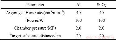
The sandwich structure of SnO2/Al/SnO2 multilayer thin films was deposited on quartz substrates with an ordinary RF sputtering system. An Al (99.99% in purity) and SnO2 (99.99% in purity) were used as the RF sputtering target. The quartz substrates were ultrasonically cleaned in acetone, ethanol and DI water for 15 min in each solution, then dried in a nitrogen atmosphere. The deposition conditions of Al and SnO2 thin films are listed in Table 1. The SnO2/Al/SnO2 multilayer films were deposited with the thickness of SnO2 about 200 nm and thickness of Al about 25 nm. As-deposited SnO2/Al/SnO2 multilayer thin films were annealed at a fix temperature of 500 °C for various annealing time of 1-8 h. The structural properties were analyzed by using the XRD with monochromatic Cu Kα radiation (λ=0.15405 nm) under operating voltage and current of 40 kV and 30 mA, respectively. The morphological studies were performed by using FE-TEM (JEOL, JEM 2100 F). The Hall-effect measurement was done at room temperature by using an HL5500PC Hall-effect measurement system. To check the reliability and repeatability of the conduction of the films, these measurements were carried out five times and concordant results were observed. The transmittance of the films was measured in the wavelength range of 400-800 nm by using an UV-vis spectrophotometer (Sinco S-4100).
Table 1 Deposition conditions of SnO2 and Al thin films

3 Results and discussion
3.1 Crystal structure and morphology
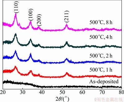
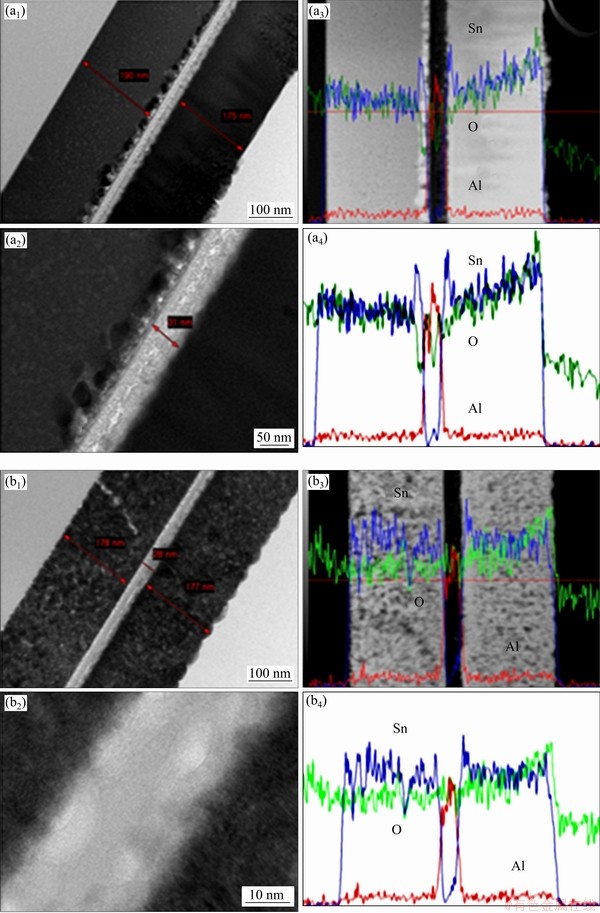
Figure 1 shows the XRD patterns of the as-deposited the SnO2(200 nm)/Al(25 nm)/SnO2(200 nm) multilayer thin films annealed for various time duration in air. It is revealed that all the thin films annealed at 500 °C have tetragonal rutile structure without any other impurity phases, which also well matches with the JCPDS card No. 41-1445. Figure 1 shows the strong orientation (110) and relatively weaker orientation (211). The intensity of the (110) plane is found to change slightly with annealing time. Figure 2 shows the FE-TEM micrographs (cross-section) of the SnO2 (200 nm)/Al(25 nm)/SnO2(200 nm) films for as deposited (Fig. 2(a1-a4)) and annealed at 500 °C for 1 h (Fig. 2(b1-b4)), respectively. The multilayer films have an average thickness ranging from 403 to 411 nm. No obvious interfaces of the Al and SnO2 layers are found in the film annealed at 500 °C for 1 h, indicating that the Al ions diffuses well into the SnO2 film [20].

Fig. 1 X-ray diffraction patterns of SnO2(200 nm)/Al(25 nm)/ SnO2(200 nm) thin films annealed for different time
3.2 Electrical properties
The effects of annealing time on the electrical properties of the multilayer films are listed in Table 2. The as-deposited SnO2/Al/SnO2 thin film has n-type conductivity. The type of conduction changes from n- type to p-type as the dominant conduction, when the film is annealed at 500 °C for 1 h. Moreover, with increasing annealing time from 1 to 8 h, the resistivity of the films increases from 1.38×100 to 6.42×10⁵ Ω・cm. When the annealing time increases above 1 h, the acceptor effect of aluminum substituting tin is activated, which results in the p-type conductivity of the films [16,21], indicating that the aluminum atoms are inactive at the amorphous state (lower grain size). The optimum annealing time for a stable p-type conducting SnO2/Al/SnO2 thin film is 1 h, with the hole concentration of 1.14×1018 cm3, and lower value of resistivity of 1.38 Ω・cm.

Fig. 2 FE-TEM cross-sectional images of as-deposited SnO2/Al/SnO2 thin film (a1-a4) and SnO2/Al/SnO2 thin film annealed at 500 °C for 1 h (b1-b4)
3.3 Optical properties
Figure 3 shows the transmittances of the SnO2/Al/ SnO2 thin films annealed for different time duration. The average transmittance of the film annealed at 500 °C for 1 h in the visible region (300-800 nm) is more than 80% with the low value of resistivity. By increasing annealing time, the films are highly transparent in the visible region and the average transmission of the films increases to over 81%. This indicates that the annealing process greatly improves the visible light transmittance of the as-deposited films. This is due to the diffusion of Al into the SnO2 layers. It is also observed that the absorption edge of the films annealed at 500 °C for 1 h shifts towards the lower wavelength region.
Table 2 Electrical properties of SnO2(200 nm)/Al(25 nm)/SnO2(200 nm) thin films annealed for different time


Fig. 3 Optical transmittance of SnO2/Al/SnO2 thin films annealed for different time
4 Conclusions
The p-type transparent conducting SnO2/Al/SnO2 thin films were prepared by RF sputtering using Al and SnO2 targets on quartz substrates. The XRD results show that the p-type conducting films possess polycrystalline SnO2 with a tetragonal rutile structure. A slight increase in the intensity of (110) plane with the annealing time is observed. Hall measurement shows that the SnO2/ Al/SnO2 multilayer films give p-type conductivity at a certain annealing temperature range of 500 °C. It is found that 500 °C, 1 h is the optimum annealing condition to get a p-type SnO2/Al/SnO2 multilayer thin films with a relatively high hole concentration (1.14× 1018 cm-3) and low resistivity (1.38 Ω・cm). The optical transmission of the SnO2/Al/SnO2 multilayer thin films is higher than 80% for the films annealed at 500 °C for 1 h.
Acknowledgements
This research was supported by the MKE (The Ministry of Knowledge Economy), Korea, under the ITRC (Information Technology Research Center) support program supervised by the NIPA (National IT Industry Promotion Agency) (NIPA-2013-H0301-13-2009). This research was financially supported by the Ministry of Education, Science Technology (MEST) and National Research Foundation of Korea (NRF) through the Human Resource Training Project for Regional Innovation (2012H1B8A2026212).
References
[1] KATAYAMA M. TFT-LCD technology [J]. Thin Solid Films, 1999, 341: 140-147.
[2] MINAMI T. Transparent conducting oxide semiconductors for transparent electrodes Semiconductor [J]. Science and Technology, 2005, 20: S35-S44.
[3] BETZ U, KHARRAZI OLSSON M, MARTHY J,  M F, ATAMNY F. Thin films engineering of indium tin oxide: Large area flat panel displays application [J]. Surface & Coatings Technology, 2006, 200: 5751-5759.
[4] FORTUNATO E, GINLEY D, HOSONO H, PAINE D C. Transparent conducting oxides for photovoltaics [J]. MRS Bulletin, 2007, 32: 242-247.
[5] GRANQVIST C G. Transparent conductors as solar energy materials: A panoramic review [J]. Solar Energy Materials, 2007, 91: 1529-1598.
[6] HOSONO H. Recent progress in transparent oxide semiconductors: Materials and device application [J]. Thin Solid Films, 2007, 515: 6000-6014.
[7] GINLEY D S, BRIGHT C. Transparent conducting oxides [J]. MRS Bulletin, 2000, 25: 15-18.
[8] YOUNG D L, MOUTINHO H, YAN Y, COUTTS T J. Growth and characterization of radio frequency magnetron sputter-deposited zinc stannate, Zn2SnO4, thin films [J]. Journal of Applied Physics, 2003, 92: 310-319.
[9] MCDOWELL M G, SANDERSON R J, HILL I G. Combinatorial study of zinc tin oxide thin-film transistors [J]. Applied Physics Letters, 2008, 92: 013502.
[10] THANGARAJU B. Structural and electrical studies on highly conducting spray deposited fluorine and antimony doped SnO2 thin films from SnCl2 precursor [J]. Thin Solid Films, 2002, 402: 71-78.
[11] MINAMI T. New n-type transparent conducting oxides [J]. MRS Bulletin, 2000, 25: 38-44.
[12] VON ROTTKAY K, RUBIN M. Optical indices of pyrolytic tin-oxide glass [J]. Materials Research Society, 1996, 426: 449-454.
[13] SINGH A K, JANOTTI A, SCHEFFLER M. Sources of electrical conductivity in SnO2 [J]. Physical Review Letters, 2008, 101: 055502.
[14] AHMED S F, KHAN S, GHOSH P K, MITRA M K, CHATTOPADHYAY K K. Effect of Al doping on the conductivity type inversion and electro-optical properties of SnO2 thin films synthesized by sol-gel technique [J]. Journal of Sol-Gel Science and Technology, 2006, 39: 241-247.
[15] MEHDI M, MOHAGHEGHI B, SAREMI M S. The influence of Al doping on the electrical, optical and structural properties of SnO2 transparent conducting films deposited by the spray pyrolysis technique [J]. Journal of Physics D: Applied Physics, 2004, 37: 1248-1253.
[16] NI J, ZHAO X, ZHENG X, ZHAO J, LIU B. Electrical, structural, photoluminescence and optical properties of p-type conducting, antimony-doped SnO2 thin films [J]. Acta Materialia, 2009, 57: 278-285.
[17] JI Z G, HE Z J, SONG Y L, LIU K, YE Z Z. Fabrication and characterization of indium-doped p-type SnO2 thin films [J]. Joural of Crystal Growth, 2003, 259: 282-285.
[18] HUANG Y X, JI Z G, CHEN C. Preparation and characterization of p-type transparent conducting tin- gallium oxide films [J]. Applied Surface Science, 2007, 253: 4819-4822.
[19] MEHDI M, MOHAGHEGHI B, SAREMI M S. Electrical, optical and structural properties of Li-doped SnO2 transparent conducting films deposited by the spray pyrolysis technique: A carrier-type conversion study [J]. Semiconductor Science and Technology, 2004, 19: 764-769.
[20] ZHAO J, ZHAO X J, NI J M, TAO H Z. Structural, electrical and optical properties of p-type transparent conducting SnO2:Al film derived from thermal diffusion of Al/SnO2/Al multilayer thin films [J]. Acta Materialia, 2010, 58: 6243-6248.
[21] GU X, ZHU L, YE Z, MA Q, HE H, ZHANG Y. Highly transparent and conductive Zn0.85Mg0.15O:Al thin films prepared by pulsed laser deposition [J]. Solar Energy Materials and Solar Cells, 2008, 92: 343-347.
退火时间对射频溅射p型透明SnO2/Al/SnO2导电薄膜结构、形貌、光学和电学性能的影响
Keun Young PARK1, Ho Je CHO1, Tae Kwon SONG1, Hang Joo KO2, Bon Heun KOO1
1. School of Materials Science & Engineering, Changwon National University, Changwon, 641-773, Korea;
2. Photovoltaic and Optoelectronic device center, Korea Photonics Technology Institute, Gwangju, 500-779, Korea
摘 要:采用SnO2和Al靶,通过射频(RF)溅射在石英基体上制备透明p型SnO2/Al/SnO2导电复合薄膜。沉积薄膜在500 °C进行不同时间(1~8 h)退火处理,研究退火时间对SnO2/Al/SnO2复合薄膜结构、形貌、光学和电学性能的影响。X射线衍射结果表明:所制备的p型导电薄膜具有四方金红石型多晶SnO2结构。霍尔效应结果显示:500 °C,1 h为最佳退火条件,该条件下SnO2/Al/SnO2复合薄膜的孔隙浓度为1.14×1018 cm-3、电阻率为1.38 Ω・cm。退火时间为1~8 h时,p型SnO2/Al/SnO2复合薄膜的光透射率可达80%以上,退火1 h时薄膜的光透射率达到最大值。
关键词:脉冲激光沉积法(PLD);透明导电氧化物(TCO);p型;多层;透射率
(Edited by Ai-hua CHEN)
Foundation item: Project (NIPA-2013-H0301-13-2009) supported by the MKE, Korea, under the ITRC support program supervised by the NIPA; Project (2012HIB8A2026212) supported by the MEST and NRF through the Human Resource Training Project for Regional Innovation, Kored
Corresponding author: Keun Young PARK; Tel: +82-55-264-5431; Fax: +82-55-262-6486; Email: bhkoo@changwon.ac.kr
DOI: 10.1016/S1003-6326(14)63299-4