
Correlation between discharging property and coatings microstructure
during plasma electrolytic oxidation
GUAN Yong-jun(πÿ”¿æ¸), XIA Yuan(œƒ ‘≠)
Institute of Mechanics, Chinese Academic of Science, Beijing100080, China
Received 19 December 2005; accepted 1 July 2006
Abstract: The voltage-current properties during plasma electrolytic discharge were determined by measuring the current density and cell voltage as functions of processing time and then by mathematical transformation. Correlation between discharge I-V property and the coatings microstructure on aluminum alloy during plasma electrolytic oxidation was determined by comparing the voltage-current properties at different process stages with SEM results of the corresponding coatings. The results show that the uniform passive film corresponds to a I-V property with one critical voltage, and a compound of porous layer and sintered ceramic particles corresponds to a I-V property with two critical voltages. The growth regularity of PEO cermet coatings was also studied.
Key words: plasma electrolytic oxidation; discharge property; voltage°™current curve; ceramic coating; aluminum alloy
1 Introduction
Plasma electrolytic oxidation (PEO) is a new technology in surface engineering[1-8]. A deep under- standing of discharge property during the process will be very helpful for revealing the mechanism of PEO and for developing new surface modification techniques based on plasma discharge in solution. However, the mechanism of plasma discharge is not clear[9-13].
In 1977, VAN et al[9] determined the current oscillogram of discharge with a stainless steel needle in sodium aluminate solution. In 2001, YANG et al[10] determined the current oscillogram of discharge with aluminum under AC condition, displaying the changes of oscillogram with processing time. In 2003, YEROKHIN et al[11] studied the size and number of discharge during PEO process using digital video imaging technology. In the same year, SUNDARARAJAN and RAMA[12] studied the size and number of discharge channels in the coatings at different processing times.
In this study, the voltage°™current properties of discharge are determined by measuring the current density and cell voltage as functions of time and then by mathematical transformation. Correlation between dis- charge I-V property and the coatings microstructure on aluminum alloy during plasma electrolytic oxidation are determined by comparing the voltage°™current properties at different processing stages with SEM results of the corresponding coatings.
2 Experimental
PEO experimental equipment is shown in Ref.[14]. The signal detection and control system contains sensors of current and voltage, digital signal gathering and processing system, and a feedback system. The response time of the current sensor is less than 1 ¶Ãs, and the response time of voltage sensor is 20-100 ¶Ãs. The signal gathering frequency is 60 kHz and the resolving power of digital system is 12 bit.
To determine the transient I-V property during discharge, voltage and current signal can be expressed as
V=V(t), I=I(t) (1)
The expression of voltage can be regarded as parametric equations of V and I with the parameter of t. The trace of the parametric equations on Cartesian coordinate of V and I represents the I-V property during plasma electrolytic discharge.
To compare the different I-V properties with and without discharge, a stainless steel plate with the same size as aluminum alloy sample was put into the same electrolyte, then AC current was past through. With the same method mentioned above, the I-V property without discharge can be determined. The method was verified by the I-V property of the aluminum alloy by passing through only cathode current.
Al-4Cu-1Mg 2024 aluminum alloy plates with the size of 22 mm°¡17 mm°¡3 mm were used as the substrate materials, and aqueous solution of sodium silicate and sodium tungstate was used as the electrolyte for PEO. Before PEO process, the samples were ground with 400# abrasive papers and cleaned with tap water. The composition of the coating was analyzed by X-ray diffraction (XRD, D/MAX-RB). The morphology of the coatings was determined by SEM.
3 Results and discussion
3.1 Characterization of current and voltage during plasma electrolytic discharge
3.1.1 Average current density and voltage
Fig.1 shows the average current density and voltage as functions of processing time. According to the voltage curve, three stages can be found in PEO process. The first is traditional anodic oxidation stage, in which the average voltage increases from 0 to about 60 V in 1 min with a luminescence on the sample surface. The second is a complex stage of continuous glow discharge and discrete micro arc discharge, in which the average voltage increases from about 60 V to about 90 V, and the increasing speed is slowed down. The third is micro arc stage, in which the average voltage increases from 90 V to about 110 V. In the late period of micro arc stage, the distribution of discharge is nonuniform and fluctuation appears on the voltage curve.
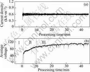
Fig.1 Changes of current density (a) and voltage (b) with processing time
3.1.2 Transient I-V property during plasma electrolytic discharge
Fig.2 shows the oscillograms of current, voltage and transient I-V property during discharge at the three stages. According to Fig.2, the peak value of current density and voltage are 8-12 mA/mm2 and 200-500 V respectively, which are much higher than the average ones as shown in Fig.1.
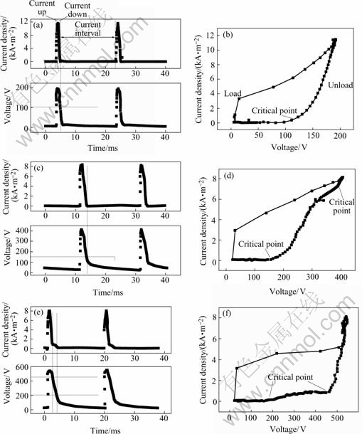
Fig.2 Oscillograms and transient I-V property during discharge: (a) and (b): First stage, processing time 30 s; (c) and (d): Second stage, processing time 5 min; (e) and ( f): Third stage, processing time 45 min
During the initial loading stage of each cycle, dV/dt increases rapidly from 9.5 V/ms(processing time 30 s) to 815 V/ms(processing time 45 min), and increases with processing time. The plasma electrolytic discharge zone is a complex four-phase system (metal-dielectric-gas-
electrolyte)[1, 11]. Because the electrical property of the four-phase system is not a pure resistance, the high increase speed of voltage at the initial stage of each cycle will make the four-phase system charge. Plasma discharge will occur if the potential reaches a certain value.
After the initial voltage-up stage of each cycle, I-V curve will descend along different lines, which shows that PEO process is irreversible. During the first stage of PEO process(the traditional anodic oxidation stage), there is only one inflexion point on the curve, and the current will be zero below this voltage. During the third stage(micro arc stage), there are two inflexion points on the curve. The second stage (the complex stage of continuous glow discharge and discrete micro arc discharge) is the transitional stage between the first and the third stages.
Fig.3 shows the transient I-V properties of discharge at different processing times in the same coordinate system. From the first stage to the second stage, the critical voltage decreases from about 230 V to 150 V, which indicates that the uniform barrier layer formed in the first stage is broken down. The decrease of I-V curve slope and the increase of critical voltage indicate the growth of the PEO coatings.
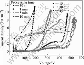
Fig.3 Transient I-V property during discharge at different PEO stages
3.1.3 Difference between I-V properties with and without discharge
During the positive current stages, the electrode is in anodic processes, and the conductive mechanism is ionic current with plasma discharge. During the negative current stages, the electrode is in cathodic processes, and the conductive mechanism is electron current without plasma discharge. To validate this point, the I-V properties of a stainless steel sample with AC current, an aluminum alloy sample with cathode current(V<0, I<0), and an aluminum alloy sample with anodic current at the beginning of PEO process (processing time 30 s ) are shown in Fig.4. Without discharge, the I-V curves are linear, passing through the origin of the coordinate. After several repeated times of PEO process as mentioned above, the I-V properties with and without discharge keep the same tendency. This indicates that the resistance of the electrolyte changes little during PEO process. So we can draw a conclusion that the impedance of the PEO electrochemistry system without discharge is a resistance and keeps constant compared with the impedance of discharge during the PEO process.
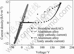
Fig.4 Comparison of different I-V properties with and without discharge
It should be noted here that the measured voltage is the dropping potential between anode and cathode which differs from the dropping potential in the exact discharge zone, but the measured I-V property during discharge can reflect the evolvement of the prepared coating.
3.2 Correlation between discharge I-V property and coatings microstructure
Fig.5 shows the surface morphologies at different processing times. In the first stage of PEO process, a Al2O3 passive film is formed on the surface rapidly as shown in Figs.4(a) and (b). In the second stage, two parallel processes occur. One is the forming of porous layer deduced by glow discharge, and the other is ceramic particles sintered by micro arc discharge. The coverage ratio of sintered ceramic particles on the surface increases in the second stage until the surface is covered thoroughly. The surface morphologies during the second stage are shown in Figs.5(c) and (d). In the third stage, the surface of sample is covered by sintered ceramic particles, and the thickness and density of the coating are increased when some micro cracks appear in the coating, as shown in Figs.5(d) and (f).
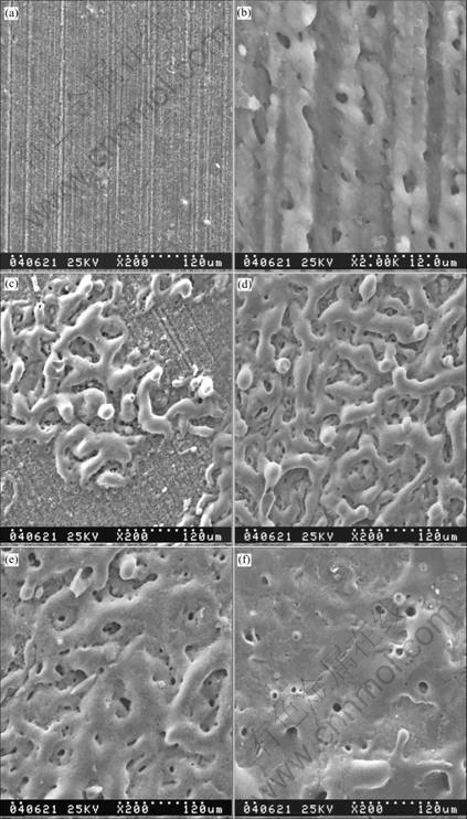
Fig.5 Surface morphologies of PEO coatings at different stages: (a) and (b) First stage; (c) and (d) Second stage; (e) and (f) Third stage
The prepared coating is one phase in the four-phase system in the discharge zone, so the coating°Øs microstructure can be indicated by the I-V properties. In the first stage, because of the forming of uniform, pore-free barrier layer, there is only one critical voltage on the I-V curve. In the second stage, transformation of barrier layer into porous layer and the forming of sintered ceramic particles lead to the decrease of critical voltage and the other critical voltage point. Being a combination of porous layer and sintered ceramic particles, the second stage is a transition stage, as shown on the I-V curves. In the third stage, sintered ceramic particles cover the sample surface completely, but the difference of microstructure in the thickness direction still exists in the coating, so two inflexion points can be seen in the I-V curves. And the appearance of micro cracks lead to the fluctuation on the average voltage curve, as shown in Fig.1. The growth of the coating leads to the increase of critical voltage and the decrease of I-V curve slope, so the I-V curves moves to the high voltage area with the processing time. The growth regularity of PEO ceramic coatings can be expressed in Fig.6, where (a) represents the first stage, (b) and (c) represent the second stage, and (d) represents the third stage.
3.3 Composition of coating
XRD pattern of PEO coatings prepared in the mixture of sodium silicate is shown in Fig,7(a), and that prepared in sodium silicate is shown in Fig,7(b). The former coating contains mullite, tungsten and amorphous phase. According to Ref.[15], coating prepared in sodium silicate is amorphous Al-Si-O. When comparing Fig.7(a) with (b), the amorphous phase in coating prepared in the mixture solution is amorphous [Al-Si-O] phase.
PEO coating prepared in sodium tungstate is WO3 [15] and that prepared in sodium silicate is amorphous Al-Si-O. While PEO process occurs in the mixed solutions of sodium silicate and sodium tungstate, on one hand, aluminum in substrate or coating deoxidizes WO3 into W, which can be indicated from the difference of Al and tungsten peaks between Figs.6(a) and (b); on the other hand, part of amorphous Al-Si-O is transformed into crystal mullite. The reactions can be express as
WO3+Al°˙W+Al2O3
Al2O3+xSiO2(1-x)Al2O3°˙yAl4.64Si1.36O9.68
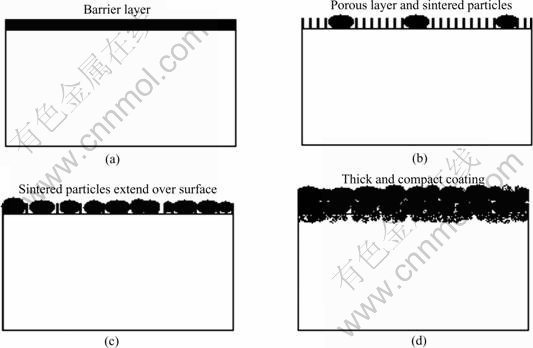
Fig. 6 Growth regularity of PEO ceramic coatings: (a) First stage; (b) and (c) Second stage; (d) Third stage
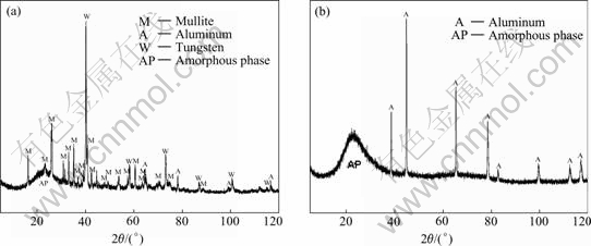
Fig.7 XRD patterns of PEO coatings prepared in different solutions: (a) Mixture of sodium silicate and sodium tungstate solution; (b) Sodium silicate solution
4 Conclusions
1) There are three different stages in PEO process, that is, anodic oxidation stage, glow and micro arc discharge and micro arc discharge stage. The I-V property during discharge can reflect the evolvement of the prepared coating. The uniform passive film corresponds to a critical voltage in I-V property, and the compound of porous layer and sintered ceramic particles correspond to two critical voltage.
2) Tungsten-containing ceramic coatings are prepared in sodium silicate and sodium tungstate by PEO process. The principal reaction is anions in the solution moving to the sample under electrical field, passing through the barrier film and reacting with the substrate in plasma discharge evolvement while high temperature induced by discharge anneals the amorphous coating into crystal phase.
References
[1] YEROKHIN A L, NIE X, LEYLAND A, MATTHEWS A, DOWEY S J. Plasma electrolysis for surface engineering [J]. Surf Coat Technol, 1999, 122: 73-93.
[2] YEROKHIN A L, VOEVODIN A A, LYUBIMOV V V, ZABINSKI J, DONLEY M. Plasma electrolytic fabrication of oxide ceramic surface layers for tribotechnical purposes on aluminium [J]. Surf Coat Technol, 1998, 110: 140-146.
[3] XUE Wen-bin, DENG Zhi-wei, CHEN Ru-yi, ZHANG Tong-he. Growth regularity of ceramic coatings formed by microarc oxidation on Al-Cu-Mg alloy [J]. Thin Solid Films, 2000, 372: 114-117.
[4] XUE Wen-bin, DENG Zhi-wei, CHEN Ru-yi, ZHANG Tong-he, MA Hui. Microstructure and properties of ceramic coatings produced on 2024 aluminum alloy by microarc oxidation [J]. Journal of Materials Science, 2001, 36: 2615-2619.
[5] GNEDENKOV S V, KHRISANFOVA O A, ZAVIDNAYA A G, SINEBRUKHOV S L, GORDIENKO P S, IWATSUBO S, MATSUI A. Composition and adhesion of protective coatings on aluminum [J]. Surf Coat Technol, 2001, 145: 146-151.
[6] NIE X, MELETIS E I, JIANG J C, LEYLAND A, YEROKHIN A L, MATTHEWS A. Abrasive wear/corrosion properties and TEM analysis of Al2O3 coatings fabricated using plasma electrolysis [J]. Surf Coat Technol, 2002, 149: 245-251.
[7] NIE X, LEYLAND A, SONG H W, YEROKHIN A L, DOWEY S J, MATTHEWS A. Thickness effects on the mechanical properties of micro-arc discharge oxide coatings on aluminium alloys [J]. Surf Coat Technol, 1999, 116-119: 1055-1060.
[8] TIAN Jun, LUO Zhuang-zi, QI Shang-kui, SUN Xiao-jun. Structure and antiwear behavior of micro-arc oxidized coatings on aluminum alloy [J]. Surf Coat Technol, 2002, 154: 1-7.
[9] VAN T B, BROWN S D, WIRTZ G P. Mechanism of anodic glow deposition [J]. Ceramic Bulletin, 1977, 56(6): 563-566.
[10] YANG Guang-liang, LU Xian-yi, BAI Yi-zhen, JIN Zeng-sun. Characterization of microarc oxidation discharge process for depositing ceramic coating [J]. Chin Phys Lett, 2001, 18(8): 1141-1143.
[11] YEROKHIN A L, SNIZHKO L O, GUREVINA N L, LEYLAND A, PILKINGTON A, MATTEWS A. Discharge characterization in plasma electrolytic oxidation of aluminium [J]. J Phys D Appl Phys, 2003, 36: 2110-2120.
[12] SUNDARARAJAN G, RAMA K L. Mechanisms underlying the formation of thick alumina coatings through the MAO coating technology [J]. Surface and Coatings Technology, 2003, 167: 269-277.
[13] TERLEEVA P, BELEVANTSEV V I, SLONOVA A I. Types of discharges in electrochemical microplasma processes [J]. Protection of Metals, 2003, 39(1): 50-54.
[14] GUAN Yong-jun, XIA Yuan. Morphous coatings deposited on aluminum alloy by plasma electrolytic oxidation [J]. Trans Nonferrous Met Soc China, 2005, 15(3): 565-570.
[15] LUKIYANCHUK I V, RUDNEV V S, ANDENKO N A, KAIDALOVA T A, PANIN E S, GORDIENKO P S. Anodic-glow oxidation of aluminum alloy in tungstate electrolytes [J]. Russian Journal of Applied Chemistry, 2002, 75(4): 573-578.
Foundation item: Project(10572141) supported by the National Natural Science Foundation of China
Corresponding author: XIA Yuan; Tel: +86-10-62554190; Fax: +86-10-62631126; E-mail: xia@imech.ac.cn
(Edited by YANG Bing)