���в㼶������������CuO@TiO2������Ĥ���Ʊ��������ˮ����
��Դ�ڿ����й���ɫ����ѧ��(Ӣ�İ�)2016���8��
�������ߣ���˧ ��ѩ�� ��� ������ ����
����ҳ�룺2094 - 2101
�ؼ��ʣ�ˮ�ֽ⣻�������������������ߣ�����ͭ����������
Key words��water splitting; photoanode; heterostructured nanowires; CuO; TiO2
ժ Ҫ��ͨ��ˮ�ȷ�Ӧ����ѧ�ƺ�֦�������������裬�Ʊ��˾��в㼶������������CuO@TiO2������Ĥ���о�������CuO@TiO2������Ĥ���ֳ����ڶ��ʺϹ���ˮӦ�õ������������ԣ���㼶���桢��չ�Ĺ�ѧ���շ�Χ�����ٵĽ�����ת�������ȡ��ڿɼ����պ�1.0 Vƫѹ(��Կ�����缫)�����£�δ���ε�TiO2������Ĥ�����Ĺ�����ܶ�Ϊ0.12 mA/cm2��CuO@TiO2������Ĥ����ͬ�����²����Ĺ�����ܶ�Ϊ0.56 mA/cm2�����ң���ʱ�������о�����CuO@TiO2������Ĥ�������õ��ȶ��ԡ���ˣ����Ʊ���CuO@TiO2������Ĥ��DZ�ڵ�̫���ܹ���ˮ�������ϡ�
Abstract: A new kind of self-standing CuO@TiO2 nanowires (NWs) film with hierarchical feature was prepared by a three-step protocol consisting of hydrothermal reaction, electroless plating, and branched growth processes. This heterostructured CuO@TiO2 NWs film demonstrates the favorable physical properties in the photoelectrochemical cell (PEC) water splitting, such as the hierarchical surface, the extended optical absorption range, and the rapid interface charge transfer kinetics. Under the illumination of the simulated solar light, the pristine TiO2 NWs film only attains a photocurrent density of 0.12 mA/cm2 at 1.0 V versus reversible hydrogen electrode (RHE). Significantly, the CuO@TiO2 NWs film can yield a dramatically increased photocurrent density of 0.56 mA/cm2 at the same applied voltage. Furthermore, amperometric I-t tests of the CuO@TiO2 NWs film reveal satisfactory stability. All the above characteristics of this heterostructured CuO@TiO2 NWs film indicate its great potential in the water splitting applications with solar visible light.
Trans. Nonferrous Met. Soc. China 26(2016) 2094-2101
Shuai ZHANG1,2, Xue-bo CAO2, Jun WU1,2, Lian-wen ZHU2, Li GU3
1. College of Chemistry, Chemical Engineering and Material Science, Soochow University, Suzhou 215123, China;
2. School of Biology and Chemical Engineering, Jiaxing University, Jiaxing 314001, China;
3. School of Materials and Textile Engineering, Jiaxing University, Jiaxing 314001, China
Received 30 December 2014; accepted 15 April 2015
Abstract: A new kind of self-standing CuO@TiO2 nanowires (NWs) film with hierarchical feature was prepared by a three-step protocol consisting of hydrothermal reaction, electroless plating, and branched growth processes. This heterostructured CuO@TiO2 NWs film demonstrates the favorable physical properties in the photoelectrochemical cell (PEC) water splitting, such as the hierarchical surface, the extended optical absorption range, and the rapid interface charge transfer kinetics. Under the illumination of the simulated solar light, the pristine TiO2 NWs film only attains a photocurrent density of 0.12 mA/cm2 at 1.0 V versus reversible hydrogen electrode (RHE). Significantly, the CuO@TiO2 NWs film can yield a dramatically increased photocurrent density of 0.56 mA/cm2 at the same applied voltage. Furthermore, amperometric I-t tests of the CuO@TiO2 NWs film reveal satisfactory stability. All the above characteristics of this heterostructured CuO@TiO2 NWs film indicate its great potential in the water splitting applications with solar visible light.
Key words: water splitting; photoanode; heterostructured nanowires; CuO; TiO2
1 Introduction
To meet the steadily increasing demand on the sustainable energy source, it is of great importance to develop novel photoanode materials in photoelectron- chemical cells (PEC) to convert solar energy into the chemical fuels by splitting water or reducing CO2 [1-3]. Among various inorganic and organic materials, metal oxides exhibit great advantages to be used as the photoanodes [4,5]. However, the performances of the photoanodes consisting of single metal oxides are usually hindered by several constraints such as the limited light absorption wavelength range, the low charge-separation efficiency, and the slow interfacial charge transfer rates. For example, the nanostructured TiO2, a n-type semiconductor serving as the benchmark of photo- electrode materials [6], is able to only utilize the light with wavelength shorter than 380 nm due to its wide band gap (3.26 eV for anatase TiO2) [7,8]. Furthermore, due to the reduced space charge layer thickness and the absence of interior electrical field in a single nanostructured material, the electron/hole injection rates from the TiO2 nanostructures into the electrolyte are governed by the kinetics of interfacial charge transfer alone, which usually leads to the growth of undesirable processes [2]. An effective approach for overcoming the above problems of the single TiO2 nanostructure is deterministically growing an additional semiconducting component on it to form the distinct heterojunction and increasing its surface complexity [5,9-13].
To date, a lot of TiO2 nanostructures, including the nanoparticle films and the nanotube/nanorods arrays have been employed as the photoanodes in PEC [14]. A comprehensive comparison of the effects of the morphologies on the performances of the TiO2 photoanodes shows that the electron diffusion coefficient in TiO2 nanorods is 200 times larger than that in nanoparticle films and the mean electron free diffusion length can reach 10 m in TiO2 nanotubes [15]. Fortunately, we have recently found that millimeter-long TiO2 NWs can be hydrothermally synthesized and spontaneously organize into a large-area free-standing film [16,17]. Moreover, since all the NWs in the film are exposed and highly accessible by foreign species, they should be particularly suitable for the deterministic growth of the secondary semiconductor. CuO, one of the few p-type semiconductors, shows a narrow band gap (1.2 eV) and diverse applications in the fields of solar energy conversion, field-emission emitters, super- conductors, optical switches, and so on [18,19]. Recently, many efforts have been directed toward the combination of this p-type semiconductor with other n-type metal oxide semiconductors to form the desirable PN junction (such as CuO@ZnO and CuO@TiO2) in order to improve the efficiencies of harvesting solar energy by encouraging the red shift and the separation of the photogenerated electrons and holes [20,21].
In this study, a new kind of self-standing CuO@TiO2 heterostructured NWs film for PEC water splitting was prepared by a three-step protocol consisting of hydrothermal reaction, electroless plating, and branched growth processes. When tested as a PEC photoanode, the CuO@TiO2 NWs film shows the optical absorption range covering the region of visible light and ultraviolet light. Under the irradiation of the simulated solar light, the CuO@TiO2 NWs film could yield a dramatically increased photocurrent density at the same applied voltage when compared with the pristine TiO2 NWs film. The CuO@TiO2 NWs film also demonstrates a much higher efficiency in the PEC water splitting than the TiO2 NWs film. The enhanced performance is attributed to the hierarchical and heterostructured features, the large red shift in the absorption spectrum, and the modified interface photocatalytic process.
2 Experimental
2.1 Preparation of self-standing CuO@TiO2 NWs film
Firstly, the self-standing TiO2 NWs film was prepared according to the previously published procedure [16,17]. After the protonation and annealing treatment at 700 ��C, the self-standing film consisting of ultra-long TiO2 NWs was formed. The growth of CuO NWs on the self-standing TiO2 NWs film was achieved by a general two-step method [22]. In the first step, the TiO2 NWs were coated by a layer of elemental Cu using electroless plating at room temperature for 30 min. The formula of the electroless bath was composed of 15 mL/L 40% formaldehyde (HCHO), 10 g/L copper sulfate (CuSO4), and 40 g/L potassium sodium tartrate (C4O6H4KNa), which play the role in the reducing agent, the copper source, and the complexing agent, respectively. In the second step, the TiO2 NWs film coated by the Cu0 layer was thermally oxidized under air atmosphere in a tube furnace. The film was heated from room temperature to 400 ��C at a rate of 2 ��C/min and held at 400 ��C for 3 h.
2.2 Characterization
The morphology characterizations of the samples were performed on a HITACHI S-4800 field emission scanning electron microscope (SEM). The phase composition of the samples was distinguished with an X��Pert PRO SUPER A rotation anode X-ray diffractometer. Optical reflection spectra of the samples were recorded on a Shimadzu 3150 UV-vis�Cnear- infrared spectrophotometer fitted with an integrating sphere. Electrochemical impedance spectroscopy (EIS) data for the samples were recorded with a Zahner Im6ex instrument under the following conditions: AC voltage amplitude 5 mV, frequency range 0.001 Hz to 100 kHz, and open circuit. The photoelectrochemical measurements were performed in a standard three-electrode cell with a quartz window (CHI Instruments, model 660C, Shanghai Chenhua, China). The TiO2 NWs film or the CuO@TiO2 NWs film, platinum wire, and Ag/AgCl were used as the working electrode, the counter electrode, and the reference electrode, respectively. A 0.5 mol/L Na2SO4 aqueous solution was used as the electrolyte. The working electrode was illuminated from the front side with the stimulated solar light emitted by a 300 W Xenon lamp through an AM 1.5G solar simulator filter. The photoelectrochemical data were collected with a CHI 660C instrument. The potential was converted to RHE potential by using the equation ��RHE=��Ag/AgCl+0.1976+ 0.059 pH.

Scheme 1 Three main steps used for growing self-standing CuO@TiO2 NWs film with hierarchical structure
3 Results and discussion
3.1 Microstructure
The free-standing CuO@TiO2 heterostructured NWs film was achieved by three main steps, as shown in Scheme 1. The first step involved the hydrothermal synthesis of the titanate film precursor and the thermal conversion of the titanate NWs film into TiO2 NWs film at the temperature of 700 ��C. In the following step, the TiO2 NWs were encapsulated by a layer of elemental Cu via the electroless plating method, which is the required raw material for growing CuO NWs. Finally, a thermal treatment step in the air atmosphere was applied to the film, which can oxidize the elemental Cu and induce the epitaxial growth of the CuO NWs.
Figure 1(a) shows the optical image of the as-prepared TiO2 NWs film with a gauze-like appearance (sizes: 1 cm �� 1 cm). The white color of the film verifies that TiO2 does not have the ability to absorb the visible light, which is the consequence of its wide band gap [19,23]. Although the film is assembled by the NWs and there only exist weak intermolecular forces among the NWs, the film is robust and is able to maintain the shape without the support of any solid substrate. This suggests that the NWs might have a large longitudinal dimension that favors the NWs to intertwine with each other. To confirm this speculation, SEM measurements of the film were performed and the results are shown in Figs. 1(b)-(d). From the panoramic view (Fig. 1(c)), an approximately periodic pattern in the film is observed, which is associated with the guided growth of the film by the ordered grooves on the side wall of the Teflon liner [17]. The SEM images of the film at the high magnification clearly reveal that the film is formed by the interconnected NWs. The lengths of the NWs can approach 1 mm and their diameters are less than 80 nm, thus showing an unprecedented high aspect ratio (>104). XRD measurements (Fig. 1(e)) demonstrate that the film is composed of anatase TiO2 (TiO2-A) and monoclinic TiO2 (TiO2-B). According to our previous study [15], TiO2-A and TiO2-B serve as the backbone and the sheath of the NWs, respectively.

Fig. 1 Optical image of self-standing TiO2 NWs film (a), SEM images of TiO2 NWs film at low magnification (b) and high magnification (c, d), and XRD pattern of TiO2 film (e)
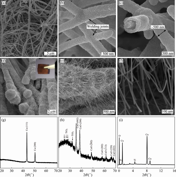
Fig. 2 SEM images of NWs film after electroless plating of copper (a-c), CuO@TiO2 NWs film (d-f), XRD patterns of NWs film after electroless plating of copper (g), CuO@TiO2 NWs film (h), and EDS spectrum of NWs film after electroless plating of copper (i)
Figures 2(a)-(c) show the SEM images of the TiO2 NWs after the electroless plating of a layer of elemental Cu. As seen, the TiO2 NWs are thickened and their surface becomes rough, indicative of the formation of the core-shell structured Cu@TiO2 NWs. In addition, the core-shell structure is exemplified by a broken nanowire at the termination (Fig. 2(c)). By comparing the diameter difference between the bare TiO2 NWs and the Cu@TiO2 NWs, the thickness of the layer of the elemental copper is determined as ~200 nm (Figs. 2(b) and (c)). During the SEM observation, we noticed that all the TiO2 NWs in the film were uniformly coated by the elemental copper, demonstrating the effectiveness of the current electroless plating method. This is because the TiO2 NWs possess a relatively broad and flat surface, which creates a comfortable nucleation and growth environment for the secondary component [10]. Interestingly, as indicated by the arrows (Fig. 2(b)), the Cu@TiO2 NWs in the film are welded together after the electroless plating. The high interconnection of the Cu@TiO2 NWs will form an efficient percolation network, which is practically advantageous for the rapid transfer of the photogenerated charges to the electrolyte interface and the back contact. Besides the evidence of the surface topography, XRD measurement also confirms the presence of the elemental copper as a primary crystalline phase in the sample (Fig. 2(g)). It is worth noting that the peaks corresponding to TiO2 NWs are missing in the XRD pattern of the sample, which implies that the component of Cu might be dominant relative to TiO2. In order to clarify the contents of Cu and Ti in the sample, EDS measurements were performed. As shown in Fig. 2(i), no impurities are detected except for the elements (Cu, O and Ti) associated with the Cu@TiO2 NWs. Quantitative analysis based on the EDS data indicates that the mole ratio of Cu to Ti is as high as 77:3, thereby supporting the XRD result.
Since the layer of the elemental copper is thick enough (~200 nm), it should provide sufficient source for growing CuO NWs via the thermal oxidation method [22]. Therefore, after the heat treatment of the Cu@TiO2 NWs at 400 ��C under air atmosphere, a large quantity of NWs were stemmed from the backbone, leading to the formation of an interesting hierarchal structure (Figs. 2(d)-(f)). Relative to the long and thick TiO2 NWs backbone, the CuO NWs are short and thin, with diameter less than 50 nm and length less than 10 ��m. More impressively, even though a series of processing steps were involved in the fabrication of hierarchal CuO@TiO2 NWs, the sample still remained the film-like appearance (inset in Fig. 2(d)). However, owing to the decoration of the CuO NWs, the color of the film has changed to brown from the initial white. We also characterized the brown film by the XRD technique (Fig. 2(h)). The result reveals that CuO and TiO2 are two primary crystalline phases of the brown film. The suppressed diffraction peaks of TiO2 relative to those of CuO is because the content of CuO is much higher than that of TiO2, as revealed by the EDS measurement as shown in Fig. 2(i). Additionally, the elemental Cu was not detected by the XRD technique, which suggests the complete transformation of the Cu@TiO2 NWs into the CuO@TiO2 NWs under the described conditions.
3.2 Optical properties
For the application of the CuO@TiO2 NWs film in the PEC device, their optical absorption properties are fundamentally important for the performance of the device. Usually, it is desired that the reflectance value is as low as possible. Figure 3 shows the surface diffuse reflection (SDR) spectra of the bare TiO2 NWs film and the CuO@TiO2 NWs film. For comparison, the SDR spectrum of CuO nanoparticles is also included in Fig. 3. As seen, bare TiO2 NWs film exhibits an intense absorption towards the light below 400 nm, which is consistent with the wide band gap of TiO2. After the growth of the CuO NWs on the TiO2 NWs, a broadened and enhanced absorption across the entire spectral range was seen. Considering that CuO shows the low reflectance characteristic in the region of visible light, the absorption enhancement of the CuO@TiO2 NWs film mainly comes from the presence of CuO NWs. Moreover, the branched surface of the NWs can also effectively diminish the reflection of the incident light, as it provides numerous scattering centers. In a word, when compared with the bare TiO2 NWs film, the CuO@TiO2 NWs film shows a large red shift and the suppressed reflection, which means that more photons can be absorbed by the film and be utilized for the subsequent PEC reaction.
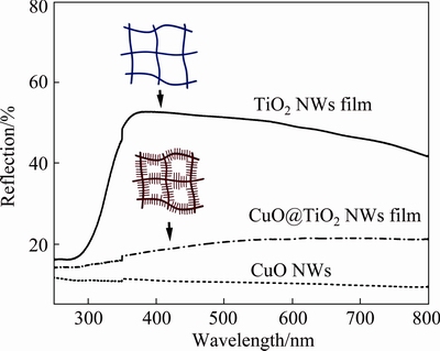
Fig. 3 Optical reflection spectra of TiO2 NWs film, CuO@TiO2 NWs film, and CuO NWs
3.3 Photoelectrochemical performance
The CuO@TiO2 NWs film was investigated as the photoanode in PECs for hydrogen generation from water splitting. PEC measurements were performed in a 0.5 mol/L Na2SO4 electrolyte solution buffered to pH 7.0 with phosphate buffer solution, by using a standard three-electrode electrochemical cell configuration. CuO@TiO2 NWs film (area: 5 mm ��5 mm), a platinum coil, and Ag/AgCl were used as the working electrode, the counter electrode, and the reference electrode, respectively. The photocurrent density versus the applied voltage curves were recorded in the dark and under the irradiation of 100 mW/cm2 of simulated solar light from a 300 W Xenon lamp through an AM 1.5G solar simulator filter (Fig. 4(a)). The photocurrent density in Fig. 4(a) was calculated based on the whole geometric area of the photoanode instead of the effective electro-active area on the photoanode. Under the dark conditions, the linear sweep voltammagrams from 0.2 to 1.2 V (versus reversible hydrogen electrode, RHE) (all potentials reported here are with respect to this reference) showed an almost negligible current in the range of 10-6 A/cm2. When the electrodes were illuminated by the standard simulated solar light, the TiO2 NWs film yielded a photocurrent density of 0.11 mA/cm2 at 1.0 V (vs RHE). With the CuO@TiO2 NWs film the photocurrent density reached 0.56 mA/cm2 at the same applied voltage, which is 6 times higher than that for the bare TiO2 NWs film. Interestingly, there is no saturation of photocurrent observed throughout the potential scan range, indicative of the efficient separation of the photo-generated charges in the CuO@TiO2 NWs [5]. Furthermore, the onset potential of the photocurrent for the CuO@TiO2 NWs film is much more negative than that for the bare TiO2 NWs film (0.51 V vs 0.78 V), which indicates that the CuO NWs grown on the surface of the TiO2 NWs have significant influence on the surface catalysis process at the semiconductor�C electrolyte interface.
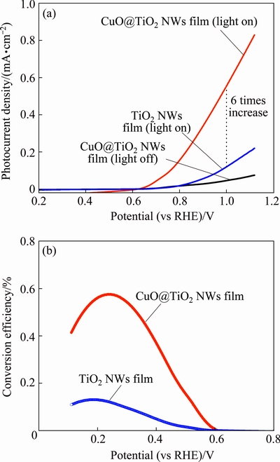
Fig. 4 J-V curves recorded for TiO2 NWs film and CuO@TiO2 NWs film with scan rate of 10 mV/s and with AM1.5G simulated solar light at 100 mW/cm2 (a) and photoconversion efficiency of TiO2 NWs film and CuO@TiO2 NWs film as function of applied potential (b)
Figure 4(b) displays the efficiency (��) of water splitting on bare TiO2 NWs film photoanode and CuO@TiO2 NWs film photoanode. The efficiency is calculated using the following equation:
 (1)
(1)
where J is the externally measured photocurrent density, Vapp is the applied voltage versus RHE, and Plight is the power density of the light [3]. As shown in Fig. 4(b), the bare TiO2 NWs film yields a maximum photoelectrode efficiency of 0.12% at the applied voltage of 0.19 V (vs RHE). In contrast, the CuO@TiO2 NWs film yields a maximum efficiency of 0.57% at the applied potential of 0.24 V (vs RHE), which is 5 times higher than that for the bare TiO2 NWs film.
To examine the PEC reaction kinetics, EIS characterizations of the TiO2 NWs film and the CuO@TiO2 NWs film were performed (Fig. 5). The insets in Fig. 5 show the corresponding equivalent circuit diagrams fitted from the EIS data. For the CuO@TiO2 NWs film, the EIS data are composed of two regions, i.e., a semicircle at high frequencies and a linear part at low frequencies (Fig. 5(a)). The charge transfer resistance of the CuO@TiO2 NWs film is around 20 �� (obtained from the x-axis intercept of semicircle), demonstrating the high charge-transfer rate between the electrolyte and the active material. As for the bare TiO 2 NWs film, the EIS data are only composed of a large semicircle and the charge transfer resistance obtained is as large as 2.1��105 ��. The sharp contrast demonstrates that the CuO@TiO2 NWs film can afford markedly faster PEC kinetics. These findings further confirm the role of the CuO NWs in the promotion of the PEC performances of the TiO2 NWs film photoanode.
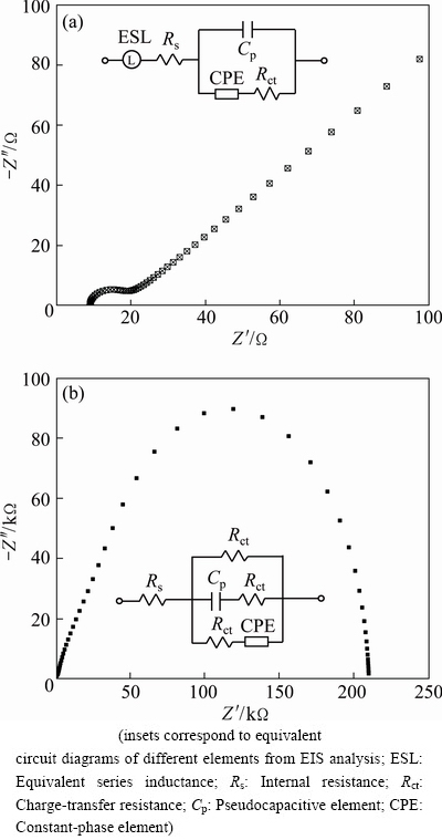
Fig. 5 Electrochemical impedance spectra of CuO@TiO2 NWs film (a) and TiO2 NWs film (b)
To assess the stability of the PECs, we also performed an amperometric I-t study on the TiO2 NWs film and the CuO@TiO2 NWs film, which were fabricated as the photoanode, under the illumination of simulated solar light at 1.0 V (vs RHE). Figure 6(a) shows the results of transient photocurrent measurements. When the stimulated solar light is switched on or switched off, a prompt and reproducible photocurrent increase or decrease was observed for both films, demonstrating the stability of the photoanode fabricated by the self-standing films. Figure 6(b) shows the photocurrent retention performance of the CuO@TiO2 NWs film. After 1200 s of operation, the attenuation of the photocurrent density is almost negligible. Consequently, the CuO@TiO2 NWs film might represent a new class of efficient, stable, and cost-effective photoanodic materials for solar water splitting.
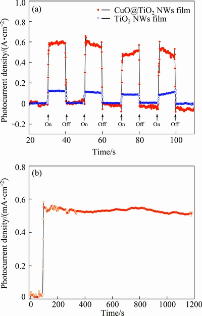
Fig. 6 Transient photocurrent density response of CuO@TiO2 NWs film and TiO2 NWs film at applied potential of 1.0 V (vs RHE) (a), and photocurrent density retention performance over 1200 s of CuO@TiO2 NWs film (b)
4 Conclusions
1) The free-standing CuO@TiO2 NWs film that exhibits the PEC water splitting activity is prepared by a three-step protocol consisting of hydrothermal reaction, electroless plating, and branched growth processes.
2) The CuO@TiO2 NWs film exhibits a significantly enhanced solar water splitting activity when compared with the bare TiO2 NWs film. Under the irradiation of the simulated solar light, the PEC photoanode made of the pristine TiO2 NWs film could attain a photocurrent density of 0.12 mA/cm2 at 1.0 V (vs RHE). At the same applied voltage, the CuO@TiO2 NWs film could yield a dramatically increased photocurrent density of 0.56 mA/cm2. Moreover, the CuO@TiO2 NWs film demonstrates a five times higher efficiency in the PEC water splitting than the TiO2 NWs film.
3) The superior PEC water splitting performance of the CuO@TiO2 NWs film is attributed to the unique architecture and the improved physical properties of the film, such as the hierarchical surface, the extended optical absorption range, and the favorable interface charge transfer kinetics.
References
[1] CHEN X B, SHEN S H, GUO L J, MAO S S. Semiconductor-based photocatalytic hydrogen generation [J]. Chemical Reviews, 2010, 110(11): 6503-6570.
[2] OSTERLOH F E. Inorganic nanostructures for photoelectrochemical and photocatalytic water splitting [J]. Chemical Society Reviews, 2013, 42: 2294-2320.
[3] WALTER M G, WARREN E L, MCKONE J R, BOETTCHER S W, MI Q X, SANTORI E A, LEWIS N S. Solar water splitting cells [J] . Chemical Reviews, 2010, 110: 6446-6473.
[4] TILLEY S D, CORNUZ M, SIVULA K, GRATZEL M. Light-induced water splitting with hematite: Improved nanostructure and iridium oxide catalysis [J]. Angewandte Chemie, 2010, 122: 6549-6552.
[5] QIU Yong-cai, YAN Ke-you, DENG Hong, YANG Shi-he. Secondary branching and nitrogen doping of ZnO nanotetrapods: building a highly active network for photoelectrochemical water splitting [J]. Nano Letters, 2011, 12: 407-413.
[6] FUJISHIMA A. Electrochemical photolysis of water at a semiconductor electrode [J]. Nature, 1972, 238: 37-38.
[7] CAO Guo-jian, CUI Bo, WANG Wen-qi, TANG Guang-ze, FENG Yi-cheng, WANG Li-ping. Fabrication and photodegradation properties of TiO2 nanotubes on porous Ti by anodization [J]. Transactions of Nonferrous Metals Society of China, 2014, 24(8): 2581-2587.
[8] DANISH R, AHMED F, ARSHI N, ANWAR M S, KOO B H. Facile synthesis of single-crystalline rutile TiO2 nano-rods by solution method [J]. Transactions of Nonferrous Metals Society of China, 2014, 24(S1): s152-s156.
[9] DLOCZIK L, ILEPERUMA O, LAUERMANN I, PETER L M, PONOMAREV E A, REDOMND G, SHAW N J, UHLENDORF I. Dynamic response of dye-sensitized nanocrystalline solar cells: Characterization by intensity-modulated photocurrent spectroscopy [J]. The Journal of Physical Chemistry B, 1997, 101: 10281-10289.
[10] CAO Xue-bo, LU Zhu-feng, ZHU Lian-wen, YANG Le, GU Li, CAI Li-ling, CHEN Jie. A new family of sunlight-driven bifunctional photocatalysts based on TiO2 nanoribbon frameworks and bismuth oxohalide nanoplates [J]. Nanoscale, 2014, 6: 1434-1444.
[11] IN S I, VAUGHN D D, SCHAAK R E. Hybrid CuO-TiO2-xNx hollow nanocubes for photocatalytic conversion of CO2 into methane under solar irradiation [J]. Angewandte Chemie International Edition, 2012, 51: 3915-3918.
[12] JUNG S, YONG K. Fabrication of CuO-ZnO nanowires on a stainless steel mesh for highly efficient photocatalytic applications [J]. Chemical Communications, 2011, 47: 2643-2645.
[13] CAO Xue-bo, CHEN Peng, GUO Yang. Decoration of textured ZnO nanowires array with CdTe quantum dots: Enhanced light-trapping effect and photogenerated charge separation [J]. The Journal of Physical Chemistry C, 2008, 112: 20560-20566.
[14] FENG X J, ZHU K, FRANK A J, GRIMES C A, MALLOUK T E. Rapid charge transport in dye-sensitized solar cells made from vertically aligned single-crystal rutile TiO2 nanowires [J]. Angewandte Chemie, 2012, 124: 2781-2784.
[15] LENG W H, BARNES P R, JUOZAPAVICIUS M, O��REGAN B C, DURRANT J R. Electron diffusion length in mesoporous nanocrystalline TiO2 photoelectrodes during water oxidation [J]. The Journal of Physical Chemistry Letters, 2010, 1: 967-972.
[16] ZHOU Yun, ZHU Lian-wen, GU Li, CAO Shu-long, WANG Li-jia, CAO Xue-bo. Guided growth and alignment of millimetre-long titanate nanofibers in solution [J]. Journal of Materials Chemistry, 2012, 22: 16890-16896.
[17] CAO Xue-bo, ZHOU Yun, WU Jun, TANG Yu-xin, ZHU Lian-wen, GU Li. Self-assembled, robust titanate nanoribbon membranes for highly efficient nanosolid capture and molecule discrimination [J]. Nanoscale, 2013, 5: 3486-3495.
[18]  G, CVELBAR U. Copper oxide nanowires: A review of growth [J]. Nanotechnology, 2012, 23: 194001.
[19] YAO Mao-hai, TANG You-gen, ZHANG Li, YANG Hai-hua, YAN Jian-hui. Photocatalytic activity of CuO towards HER in catalyst from oxalic acid solution under simulated sunlight irradiation [J]. Transactions of Nonferrous Metals Society of China, 2010, 20(10): 1944-1949.
[20] LIU Z Y, BAI H W, SUN D D. Hierarchical CuO/ZnO membranes for environmental applications under the irradiation of visible light [J]. International Journal of Photoenergy, 2011, 2012: 804840.
[21] LI G H, DIMITRIJEVIC N M, CHEN L, RAJH T, GRAY K A. Role of surface/interfacial Cu2+ sites in the photocatalytic activity of coupled CuO-TiO2 nanocomposites [J]. The Journal of Physical Chemistry C, 2008, 112: 19040-19044.
[22] JIANG Xu-chuan, HERRICKS T, XIA You-nan. CuO nanowires can be synthesized by heating copper substrates in air [J]. Nano Letters, 2002, 2: 1333-1338.
[23] WU N Q, WANG J, TAFEN D N, WANG H, ZHENG J G, LEWIS J P, LIU X G, LEONARD S S, MANIVANNAN A. Shape-enhanced photocatalytic activity of single-crystalline anatase TiO2 (101) nanobelts [J]. Journal of the American Chemical Society, 2010, 132: 6679-6685.
�� ˧1,2����ѩ��2, �� ��1,2��������2���� ��3
1. ���ݴ�ѧ �����뻯ѧ����ѧ�������� 215123��
2. ����ѧԺ �����뻯ѧ����ѧԺ������ 314001��
3. ����ѧԺ �������֯����ѧԺ������ 314001
ժ Ҫ��ͨ��ˮ�ȷ�Ӧ����ѧ�ƺ�֦�������������裬�Ʊ��˾��в㼶������������CuO@TiO2������Ĥ���о�������CuO@TiO2������Ĥ���ֳ����ڶ��ʺϹ���ˮӦ�õ������������ԣ���㼶���桢��չ�Ĺ�ѧ���շ�Χ�����ٵĽ�����ת�������ȡ��ڿɼ����պ�1.0 Vƫѹ(��Կ�����缫)�����£�δ���ε�TiO2������Ĥ�����Ĺ�����ܶ�Ϊ0.12 mA/cm2��CuO@TiO2������Ĥ����ͬ�����²����Ĺ�����ܶ�Ϊ0.56 mA/cm2�����ң���ʱ�������о�����CuO@TiO2������Ĥ�������õ��ȶ��ԡ���ˣ����Ʊ���CuO@TiO2������Ĥ��DZ�ڵ�̫���ܹ���ˮ�������ϡ�
�ؼ��ʣ�ˮ�ֽ⣻�������������������ߣ�����ͭ����������
(Edited by Xiang-qun LI)
Foundation item: Projects (21107032, 21473079) supported by the National Natural Science Foundation of China. Projects (Y201330088, Y20133003) supported by the Department of Education of Zhejiang Province, China
Corresponding author: Li GU; Tel/Fax: +86-573-83643022; E-mail: guli@mail.zjxu.edu.cn
DOI: 10.1016/S1003-6326(16)64324-8

