高硅SiCp/Al复合材料化学镀Ni-P合金层及其生长动力学
来源期刊:中国有色金属学报(英文版)2016年第3期
论文作者:方萌 胡玲 杨磊 史常东 吴玉程 汤文明
文章页码:799 - 805
关键词:SiCp/Al复合材料;化学镀;Ni-P合金膜;显微结构;生长动力学
Key words:SiCp/Al composite; electroless plating; Ni-P alloy film; microstructure; growth kinetics
摘 要:经Sn/Pd活化后,在SiC体积分数为65%的SiCp/Al复合材料表面化学镀Ni-P合金,研究复合材料表面形貌及其对Ni-P沉积过程的影响,以及Ni和P原子间的结合方式。结果表明,Sn/Pd活化点分布不均导致Ni-P颗粒优先沉积在Al合金和粗糙的SiC表面以及腐蚀孔洞中,Ni-P 合金膜具有非晶结构,其中Ni原子和P原子间依靠化学键结合。在形成连续的Ni-P合金膜之后,化学镀Ni-P合金不再受SiCp/Al复合材料表面形貌及特性的影响,而是受化学镀本身控制,Ni-P合金膜遵循线性生长动力学,其活化能为68.44 kJ/mol。
Abstract: After Sn/Pd activating, the SiCp/Al composite with 65% SiC (volume fraction) was coated by electroless Ni-P alloy plating. Surface morphology of the composite and its effect on the Ni-P alloy depositing process and bonding action of Ni and P atoms in the Ni-P alloy were studied. The results show that inhomogeneous distribution of the Sn/Pd activating points results in preferential deposition of the Ni-P alloy particles on the Al alloy and rough SiC particle surfaces and in the etched caves. The Ni-P alloy film has an amorphous structure where chemical bonding between Ni and P atoms exists. After a continuous Ni-P alloy film formed, electroless Ni-P alloy plating is not affected by surface morphology and characteristics of the SiCp/Al composite any longer, but by the electroless plating process itself. The Ni-P alloy film follows linear growth kinetics with an activation energy of 68.44 kJ/mol.
Trans. Nonferrous Met. Soc. China 26(2016) 799-805
Meng FANG1, Ling HU2, Lei YANG2, Chang-dong SHI2, Yu-cheng WU3, Wen-ming TANG1,3
1. School of Materials Science and Engineering, Hefei University of Technology, Hefei 230009, China;
2. 43 Institute, China Electronics Technology Group Corporation, Hefei 230088, China;
3. Key laboratory of Functional Materials and Devices of Anhui Province, Hefei University of Technology, Hefei 230009, China
Received 29 April 2015; accepted 20 October 2015
Abstract: After Sn/Pd activating, the SiCp/Al composite with 65% SiC (volume fraction) was coated by electroless Ni-P alloy plating. Surface morphology of the composite and its effect on the Ni-P alloy depositing process and bonding action of Ni and P atoms in the Ni-P alloy were studied. The results show that inhomogeneous distribution of the Sn/Pd activating points results in preferential deposition of the Ni-P alloy particles on the Al alloy and rough SiC particle surfaces and in the etched caves. The Ni-P alloy film has an amorphous structure where chemical bonding between Ni and P atoms exists. After a continuous Ni-P alloy film formed, electroless Ni-P alloy plating is not affected by surface morphology and characteristics of the SiCp/Al composite any longer, but by the electroless plating process itself. The Ni-P alloy film follows linear growth kinetics with an activation energy of 68.44 kJ/mol.
Key words: SiCp/Al composite; electroless plating; Ni-P alloy film; microstructure; growth kinetics
1 Introduction
In recent years, SiCp/Al composites with high SiC volume fraction have been widely used in electronics packaging thermal sinks and carriers due to their excellent properties of low coefficient of thermal expansion, high thermal conductivity, high specific modulus and so on [1-4]. However, high volume SiCp/Al composites can not be soldered directly with metal leads, such as Kovar and Cu. Therefore, surface metallization of the composites is needed before soldering. Considering large amounts of dielectric SiC particles in the composites, electroless plating of Ni-P alloy film is usually implemented to form a conductive priming coating for subsequently electroplating Ni and Au bi-layer on the SiCp/Al composites [5-7].
As for research on electroless Ni-P alloy plating on the SiCp/Al composites,  et al [8] have determined that it is not the same for the Ni-P alloy depositing on large SiC particle, Al alloy and small SiC particle zone. Without Sn/Pd activating, the Ni-P alloy film deposited on large SiC particles has a lower continuity, compared with that on Al alloy or small SiC particles. LI et al [9] found that the initial Ni-P alloy plating prefers to occur at the SiCp/Al interface than elsewhere in an acid plating bath. LI et al [10] reported that re-crystallization of Ni at the interface between the Ni-P alloy film and the SiCp/Al composites takes place to form an atomic bonding between the Ni-P alloy film and the composite substrate. Although study on electroless Ni-P alloy plating on high volume SiCp/Al composites is essentially important, published literatures on this issue are still limited so far, effects of surface morphology of the composites and Sn/Pd activation on the electroless Ni-P alloy plating process have not been reported yet. And, only little research on the growth kinetics of electroless Ni-P alloy plating on high volume SiCp/Al composites has been published. Therefore, a more detailed examination of the plating process and growth kinetics of electroless Ni-P alloy plating on the composites is required.
In this work, the high volume SiCp/Al composite with 65% SiC (volume fraction) was chosen to fulfill electroless Ni-P alloy plating. Morphologies of the original, Sn/Pd activating and electroless plating surfaces of the composite were observed, respectively. Growth kinetics of the Ni-P alloy film on the SiCp/Al composite was also investigated.
2 Experimental
SiCp/Al composite with 65% SiC fabricated through a pressureless infilitration technique was selected as the substrate material. After surface grinding, the substrate was cut into thin sheets of 70 mm × 50 mm × 1.5 mm in size. The sheets were ultrasonically cleaned in acetone for 10 min. The sheet samples were then sensitized by dipping in a SnCl2+HCl aqueous solution for 1 min, and activated by dipping in a PdCl2+HCl aqueous solution for 30 s. The samples were rinsed with deionized water after each step.
Concentration of the acidic plating bath with a pH value of 5.0 employed in this study is listed in Table 1, which stays the same in the whole electroless plating process. After Sn/Pd activating, the SiCp/Al composite specimens were immediately dipped in the 362 K plating bath for 3, 10, 20, 40 and 60 min, respectively, in order to investigate the depositing process in detail. In addition, the SiCp/Al composite specimens were also deposited in the same plating baths at different temperatures of 343, 353, 358 K for various time of 10, 20, 40 and 60 min, respectively, for measuring the thicknesses of Ni-P alloy films formed at varied plating parameters. And then, the electroless plating kinetics of Ni-P alloy on the high volume SiCp/Al composite was investigated.
Table 1 Concentration of electroless Ni-P alloy plating bath

Surface morphology and elemental composition of the samples with or without electroless Ni-P alloy plating were examined using a JSM-6490LV scanning electron microscope (SEM) equipped with an Oxford INCA energy dispersive X-ray detector (EDS). The accelerate voltage is 20 kV and the secondary electron imaging methods were used. Cross-sectional view of the electroless Ni-P alloy deposit was also observed by SEM. Crystal structure of the Ni-P alloy was identified using a D/MAX2500V copper (Kα1=1.5418  ) rotating anode X-ray diffractometer (XRD). The XRD analysis was conducted at 20 kV and 200 mA with a scanning speed of 2 (°)/min. An ESCALAB250 X-ray photo- electron spectroscopy (XPS) was employed to test the surface electronic states of the initial Ni-P alloy deposit. After electroless plating at different temperatures for various time, the SiCp/Al composite samples were cross-sectioned, mounted in epoxy resin and ground with 280, 500 and 800 grit SiC abrasive papers successively, then polished with 2.5 mm diamond paste in cold water. Finally, the thickness of the Ni-P alloy deposit was directly measured from the SEM cross-sectional images of the Ni-P alloy film.
3 Results and discussion
3.1 Surface morphologies of SiCp/Al composite with or without Sn/Pd activating
As shown in Fig. 1(a), after grinding, surface morphology of the composite is complicated. SiC particle surface peels off in a cleavage mode, leaving high-density small shallow holes and large smooth fracture surfaces. On the other hand, there are lots of fine honeycomb-like holes on Al alloy surface. After Sn/Pd activating, Sn/Pd points preferentially aggregate on the rough Al alloy and SiC particle surfaces. The points on the smooth SiC particle surface are small in amount (Fig. 1(b)). Moreover, after activating, there are some caves on the composite surface, especially at the SiCp/Al interface, formed by the corrosion of the Al alloy by HCl in the sensitizing solution. In these caves, there are lots of Sn points, some big Sn points are about 1 μm in diameter; however, most of them are too tiny to be identified in Fig. 1(c). Therefore, after Sn/Pd activating, the Sn/Pd points apparently distribute inhomogeneously, which have a great effect on the electroless Ni-P alloy plating on the composite surface.
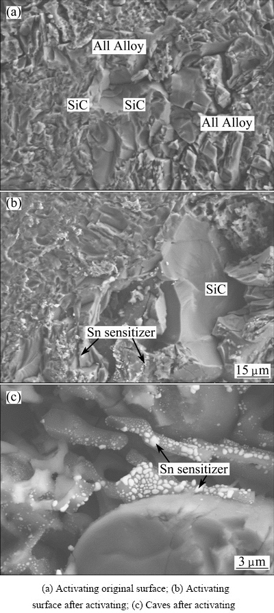
Fig. 1 Planar SEM images of SiCp/Al composite surface with or without Sn/Pd
3.2 Formation and growth of electroless Ni-P alloy deposit
Figure 2 shows surface morphologies of the SiCp/Al composite specimens after depositing Ni-P alloy at 362 K for various time. After plating for 3 min, it can be seen that lots of tiny spherical Ni-P particles exist on the specimen surface; however, their distribution is inhomogeneous. Ni-P alloy particles are sparsely dispersed on the smooth SiC particle surface. Meanwhile, the Ni-P alloy particles nearly distribute in a continuous state on the Al alloy and rough SiC particle surfaces and at the SiCp/Al interface (Fig. 2(a)), indicating that the Ni-P particles prefer to deposit at the locations rich in Sn/Pd activating points in Fig. 1. The result is also consistent with that reported by MATRON and SCHLESINER [11]. In their study, the Ni-P alloy particles preferentially deposit on the Sn/Pd activating points on the glass surface and grow in an insular mode. This phenomenon implies that the initial deposition of the Ni-P alloy is related to the presence of Pd, because the Pd particles act as charge exchange and hydrogen evolution centers to offer the electrons for Ni ions to be reduced to Ni metal. As the electroless plating time increases, the Ni-P particles cover the Sn/Pd points completely. Next, they act as new activating points, instead of the Sn/Pd ones, to catalyze the electroless depositing reaction and grow in the horizontal and vertical directions to the composite substrate surface. Because Ni has the same face center cubic (FCC) structure and the similar lattice constant as Al, the Ni atoms deposited on the Al alloy surface in the SiCp/Al composite can grow epitaxially along the Al crystal lattice orientation and then gradually transfer to the Ni crystal lattice orientation via a dislocation mechanism [12]. Therefore, interface bonding between the deposited Ni-P alloy film and the Al alloy is strong. On the contrary, crystal structure and lattice constant of Ni are quite different with those of SiC, the Ni atoms only grow on the Sn/Pd activating points or among these points on the SiC particle surface. And, interface bonding between the deposited Ni-P alloy film and SiC is rather weak. Although the depositing rate of Ni-P alloy on the SiC particle surface is low, a continuous Ni-P alloy film can also be formed at last, with prolonging the electroless plating time (Fig. 2(b)).
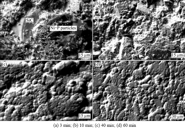
Fig. 2 Surface morphologies of Ni-P alloy films after plating at 362 K for various time
After electroless plating for 10 min, more SiC particles are covered by the Ni-P alloy; however, roughness of the Ni-P alloy film is very high, especially in the holes of the SiCp/Al composites. Fortunately, the Ni-P alloy has a larger depositing rate, due to the high-density Sn/Pd points in the holes (Fig. 1(c)). Moreover, the holes have high surface roughness, which is also beneficial to improvement of the depositing rate of the Ni-P alloy [13]. Roughness of the Ni-P alloy film is therefore decreased with prolonging the plating time. Meanwhile, the Ni-P alloy cellulars, composed of Ni-P alloy grains, grow, resulting in gradual elimination of the intervals among them and thus improvement of the density of the deposited Ni-P alloy film (Figs. 2(b) and (c)). Finally, a dense, continuous and smooth Ni-P alloy film should be formed on the high volume SiCp/Al composite after depositing for 60 min (Fig. 2(d)). Fracture surface view of the Ni-P alloy film is shown in Fig. 3(a). The Ni-P alloy film is dense, smooth and approximately uniform in thickness and contacts tightly with the SiCp/Al composite substrate no matter on the Al alloy surface or on the SiC particle surface. However, on the Al alloy surface, the film is slightly thicker, and the Ni-P alloy cellulars are larger, possibly due to larger Sn/Pd activating points over there than those on the SiC particle surface, especially on the smooth SiC particle surface. EDS analysis determines that the composition of Ni-P films is about 12.76% P (Fig. 3(b)).
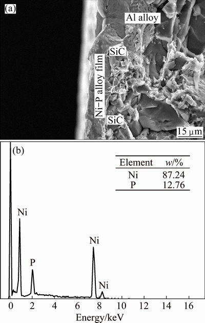
Fig. 3 SEM fracture surface image (a) and planar EDS spectrum (b) of SiCp/Al composite electroless Ni-P alloy plated at 362 K for 60 min
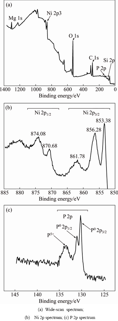
Fig. 4 XPS spectra of SiCp/Al composite after electroless Ni-P alloy plated at 362 K for 3 min
3.3 Atom bonding and structure of Ni-P alloy deposit
As shown in Fig. 4(a), except Si 2p, C 1s and Mg 1s peaks originated from the SiCp/Al composite, Ni 2p and P 2p peaks were also detected in the XPS spectrum. In Fig. 4(b), three main Ni 2p binding energy (BE) peaks are located at BE1=(853.3±0.1) eV, BE2=(856.2±0.1) eV and BE3=(861.7±0.1) eV, respectively. Compared with the standard binding energy of Ni 2p3/2 in Table 2, the Ni 2p BE1 peak refers to the binding energy peak of Ni metal, which is intensive and has a full width at half maximum (FWHM) of 1.1 eV. The Ni 2p BE2 peak refers to the binding energy peak of Ni compounds of NiO, Ni2O3 and/or Ni(OH)2, which has a high FWHM (about 3.7 eV). The formation of Ni oxides attributes to oxidation of the Ni-P alloy film when exposed in air. The Ni 2p BE3 peak has a FWHM of about 5.7 eV and a rather low intensity. OLIVEIRA and do REGO [14] considered that it generated through the interaction between the unpaired electrons of Ni0 and Ni2+. Therefore, it refers to the binding energy peak of mixture of the Ni metal and the Ni compounds mentioned above.
Table 2 Standard binding energies of Ni and P in different states [15,16]
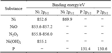
Specifically, the binding energies of Ni metal were detected to be 870.68 eV (Ni 2p1/2) and 853.38 eV (Ni 2p3/2), respectively (Fig. 4(b)). Here, Ni 2p1/2 and Ni 2p3/2 represent the two 2p electron orbits of Ni atom decided by different inner quantum number, respectively, the same as P 2p1/2 and P 2p3/2 hereinafter. Compared with the standard binding energies of Ni metal, i.e., (870.0±0.1) eV (Ni 2p1/2) and (852.7±0.1) eV (Ni 2p3/2), a 0.68 eV positive chemical shift can be determined for the Ni 2p1/2 and Ni 2p3/2 binding energy peaks in the deposited Ni-P alloy. Similarly, the binding energies of P atoms in the Ni-P alloy are 131.08 eV (P 2p1/2) and 130.28 eV (P 2p3/2), respectively. Compared with the standard binding energies of P elementary substance, i.e., 131.4 eV (P 2p1/2) and 130.6 eV (P 2p3/2) [15], there is a 0.32 eV negative chemical shift for these two P 2p binding energy peaks in Fig. 4(c). It can be explained that during co-depositing Ni and P atoms on the SiCp/Al composite, partial overlapping of the Ni and P electron clouds occurs, resulting in decrease/increase of the outer electron cloud density. Binding energy peaks of Ni and P shifting in reverse direction imply increase/ decrease of the inner electronic binding energy of Ni/P atoms in the Ni-P alloy. This means that parts of Ni atoms and P atoms have constructed a chemical bonding during the Ni-P alloy co-deposition process. According to research of LI et al [2], no positive shift, but the shift towards the minus direction of the binding energy of Ni electron was detected, indicating a bonding action between Ni atoms from the Ni-P alloy deposits and Al atoms from the SiCp/Al composites and gain of electrons for Ni atoms during the bonding process. On the whole, in the initial electroless Ni-P alloy plating process, chemical bonding between Ni atoms and P atoms in the Ni-P alloy deposit and that between Ni atoms and the SiCp/Al composite substrate both generate. Because chemical shifts of the Ni and P binding energies are both less than 1 eV, the chemical bonding between Ni and P atoms may be a mixture of covalent and ionic bondings [10]. A solid solution alloy of P in Ni is therefore formed in the initial electroless plating of Ni-P alloy on the high volume SiCp/Al composite.
In order to confirm structural characterization of the electroless plated Ni-P solid solution alloy, XRD analysis of the samples was carried out, as shown in Fig. 5. In the XRD pattern of the sample deposited for 3 min, except the diffraction peaks of SiC, Al and Si from the composite substrate, the Ni-P alloy diffraction peak could be detected. It locates near 2θ=45°, which is bread-like in shape with a low intensity. Such a bread-like diffraction peak is more apparent in the XRD pattern of the sample deposited for 60 min, indicating that the electroless plated Ni-P alloy is amorphous. It has been determined that only amorphous Ni-P solid solution structure can be formed for the alloy with a high P composition (>10%) [17,18]. The Ni-P alloy has a P content of 12.76% (Fig. 3(b)), so it has an amorphous structure, accordingly.
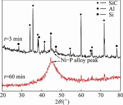
Fig. 5 XRD patterns of SiCp/Al composite after electroless Ni-P alloy plated at 362 K for 3 min and 60 min
3.4 Growth kinetics of electroless plated Ni-P alloy film
In general, growth rate of the electroless plated Ni-P alloy film, v, is an exponential function of the plating temperature, T, in the condition of the plating bath having unchangeable concentration during the depositing process:
v=Kexp[-Ea/(RT)] (1)
where Ea and K are activation energy and rate constant of the electroless plating process, respectively, R is mole gas constant. By taking logarithm of Eq. (1), Eq. (2) can be obtained:
lg v=K′-Ea/(2.3R)・1/T (2)
Electroless Ni-P alloy plating can be divided into two sub-processes: one is diffusion of Ni2+, H2PO2- and other ions from the plating bath to the deposited surface; the other is redox reactions among these ions and Sn/Pd activating points to form Ni and P atoms co-deposited on the substrate surface.
As shown in Fig. 6, at the setting temperature of the plating bath, a linear relationship between the thickness of the Ni-P alloy film and the depositing time is approximately followed, showing that the electroless Ni-P alloy plating on the high volume SiCp/Al composite is not controlled by the ion diffusion, but by the ion redox-reaction process. Because the electroless plating process takes place at relatively high temperature, diffusion rate of the ions in the plating bath is fast. As a result, the ions diffused from the plating bath to the depositing surface exceed those consumed by the Ni-P alloy co-depositing reactions. In addition, during the electroless plating process, the consumed ions are compensated immediately to ensure the constant ion concentration in the plating bath, in this situation, the ion diffusion can be treated as a steady state process, which is described in an equation: ?Ci/?t=0 [19]. So, the supplement of ions for the electroless plating is always sufficient. Thus, it is concluded that the reaction between Ni2+ and H2PO2- to form Ni and P co-depositing is the rate controlled step for electroless Ni-P alloy plating on the high volume SiCp/Al composite.
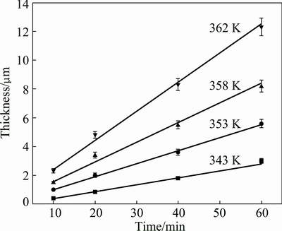
Fig. 6 Plots of thickness of Ni-P alloy film vs time at different plating temperatures
In this work, the growth rates of the electroless plated Ni-P alloy film at different temperatures are calculated to be 0.04 mg/(cm2・min) (0.05 μm/min) at 343 K, 0.07 mg/(cm2・min) (0.09 μm/min) at 353 K, 0.1 mg/(cm2・min) (0.1 μm/min) at 358 K and 0.2 mg/(cm2・min) (0.2 μm/min) at 362 K, respectively. Based on Figs. 6 and 7, activation energy for the electroless Ni-P alloy plating on the high volume SiCp/Al composite is then calculated to be 68.44 kJ/mol. According to LIN and LONG [20], the activation energy mainly refers to the energy for growth, not for nucleation of the Ni-P alloy film. This value is very close to 66.9 kJ/mol, the activation energy for electroless Ni-P alloy plating on the Si substrate [21]. In summary, the initial electroless Ni-P alloy plating is dramatically affected by surface morphology and characteristics of the SiCp/Al composite. However, once a continuous Ni-P alloy film is formed after plating for 10 min, the influence of surface morphology of the composite substrate nearly disappears. The growth of the Ni-P alloy film only depends on the electroless Ni-P alloy plating process itself, and has nothing to do with the SiCp/Al composite substrate.
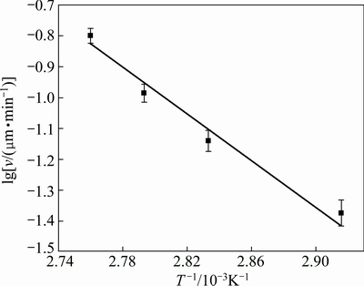
Fig. 7 Plot of growth rate of Ni-P alloy film vs temperature
4 Conclusions
1) Due to inhomogeneous distribution of Sn/Pd activating points, electroless Ni-P alloy plating on the high volume SiCp/Al composite is not uniform in the initial stage. The electroless Ni-P alloy plating on the Al alloy and rough SiC particle surfaces and in the caves at the SiCp/Al interface is much rapider than that on the smooth SiC particle surface. As the plating time increases, a continuous Ni-P alloy film forms on the composite surface via the planar and/or epitaxial growth mechanisms.
2) During electroless Ni-P alloy plating on high volume SiCp/Al composite, chemical bonding between Ni and P atoms generates to form a solid solution of P in Ni. The Ni-P alloy film is amorphous due to serious Ni lattice distortion in the Ni-P alloy with a high P content.
3) Growth of the Ni-P alloy film on the high volume SiCp/Al composite follows a linear kinetics with activation energy of 68.44 kJ/mol. The electroless Ni-P alloy plating process is controlled by the ion redox-reaction on the SiCp/Al composite surface. Once a continuous Ni-P alloy film is formed, the electroless Ni-P alloy plating process is not affected by morphology and characteristics of the SiCp/Al composite any longer.
References
[1] LIU Mei-tan, CAI Xu-sheng, LI Guo-qiang. Microstructure and thermal properties of high-performance SiC reinforced Al matrix composite [J]. The Chinese Journal of Nonferrous Metals, 2013, 23(4): 1040-1046. (in Chinese)
[2] LI Li-bo, AN Mao-zhong, WU Gao-hui. Model of electroless Ni deposition on SiCp/Al composites and study of the interfacial interaction of coatings and substrate surface [J]. Applied Surface Science, 2005, 252: 959-965.
[3] WANG Shu-yan, SI Nai-chao, XIA Yong-ping, LI Liu. Influence of nano-SiC on microstructure and property of MAO coating formed on AZ91D magnesium alloy [J]. Transactions of Nonferrous Metals Society of China, 2015, 25(6): 1926-1934.
[4] ZHU Xiao-min, YU Jia-kang, WANG Xin-yu. Microstructure and properties of Al/Si/SiC composites for electronic packaging [J]. Transactions of Nonferrous Metals Society of China, 2012, 22(7): 1686-1692.
[5] QIN Tie-nan, MA Li-qun, YAO Yan, NI Cong, ZHAO Xiang-yu, DING Yi. An in situ measure method to study deposition mechanism of electroless Ni-P plating on AZ31 magnesium alloy [J]. Transactions of Nonferrous Metals Society of China, 2011, 21(12): 2790-2797.
[6] QI Zu-qiang, LU Wan-jia, GUO Ai-qing, HU Yong, LEE Wei-ming. Investigation on circular plating pit of electroless Ni-P coating [J]. Industrial & Engineering Chemistry Research, 2014, 53: 3097-3104.
[7] WU Mao, QU Xuan-hui, HE Xin-bo, REN Shu-bin, QIN Ming-li. Interfacial reactions between Sn-2.5Ag-2.0Ni solder and electroless Ni(P) deposited on SiC/Al composites [J]. Transactions of Nonferrous Metals Society of China, 2010, 20(6): 958-965.
[8]  A, UTRILLA M V, RAMS J, RODRIGO P, FERRER M J. Electroless multilayer coatings on aluminum-silicon carbide composites for electronics packaging [J]. Journal of the European Ceramic Society, 2007, 27: 3983-3986.
[9] LI Jian-zhong, TIAN Yan-wen, LI Ying, WANG Xiang-rong. Process of Ni-P electroless deposition on SiCp/Al composites from acid bath [J]. Advanced Materials Research, 2011, 160: 314-318.
[10] LI Li-bo, AN Mao-zhong, WU Gao-Hui. Study on adhesion mechanism of SiCp/Al composites and electroless nickel coating [J]. Chinese Journal of Inorganic Chemistry, 2005, 21: 983-986. (in Chinese)
[11] MATRON J P, SCHLESINER M. The nucleation, growth and structure of thin Ni-P films [J]. Journal of Electrochemical Society, 1968, 115: 16-21.
[12] XU Bin-shi, ZHU Shao-hua, LIU Shi-can. Materials surface engineering [M]. 1st ed. Harbin: Harbin Institute of Technology Press, 2005. (in Chinese)
[13] VITRY V, KANTA A F, DELAUNOIS F. Initial and formation of electroless nickel-boron coatings on mild steel: Effect of substrate roughness [J]. Materials Science and Engineering B, 2010, 175: 266-273.
[14] OLIVEIRA C M, do REGO D A M B. The effect of the hypophosphite ion oxidation on the Ni surface electrode―An XPS study [J]. Journal of Alloys and Compound, 2006, 425: 64-68.
[15] VINCENT C B. Handbook of monochromatic XPS spectra [M]. USA: Wiley, 2000.
[16] KUHLENBECK H,  R, JAEGER G, ILLING G, MENGES M, MULL T, FREUND H J. Molecular absorption on oxide surface: Electronic structure and orientation of NiO on NiO(100)/Ni(100) and on NiO(100) as determined from electron spectroscopies and ab initio cluster calculations [J]. Physical Review B, 1991, 43: 1969-1985.
[17] HENTSCHEL T, ISHEIM D, KIRCHHEIM R,  F, KREYE H. Nanocrystalline Ni-3.6 at.% P and its transformation sequence studied by atom-probe field-ion microscopy [J]. Acta Materialia, 2000, 48: 933-941.
[18] WANG Hui-long, LIU Ling-yun, JIANG Wen-feng. Effect of novel ternary ligand system on acidic electroless Ni-P plating on AZ91D magnesium alloy [J]. Transactions of Nonferrous Metals Society of China, 2014, 24(9): 3014-3022.
[19] CHA Quan-xing. Introduction to dynamics of electrode process [M]. 3rd ed. Beijing: Science Press, 2004. (in Chinese)
[20] LIN K L,LONG C S. The deposition behaviour of electroless nickel on alumina substrate [J]. Materials Chemistry and Physics, 1993, 35: 53-57.
[21] LIU W L, HSIEH S H, TSAI T K, CHEN W J, WU S S. Temperature and pH dependence of the electroless Ni-P deposition on silicon [J]. Thin Solid Films, 2006, 510: 102-106.
方 萌1,胡 玲2,杨 磊2,史常东2,吴玉程3,汤文明1,3
1. 合肥工业大学 材料科学与工程学院,合肥 230009;
2. 中国电子科技集团公司 第四十三研究所,合肥 230088;
3. 合肥工业大学 先进功能材料与器件安徽省重点实验室,合肥 230009
摘 要:经Sn/Pd活化后,在SiC体积分数为65%的SiCp/Al复合材料表面化学镀Ni-P合金,研究复合材料表面形貌及其对Ni-P沉积过程的影响,以及Ni和P原子间的结合方式。结果表明,Sn/Pd活化点分布不均导致Ni-P颗粒优先沉积在Al合金和粗糙的SiC表面以及腐蚀孔洞中,Ni-P 合金膜具有非晶结构,其中Ni原子和P原子间依靠化学键结合。在形成连续的Ni-P合金膜之后,化学镀Ni-P合金不再受SiCp/Al复合材料表面形貌及特性的影响,而是受化学镀本身控制,Ni-P合金膜遵循线性生长动力学,其活化能为68.44 kJ/mol。
关键词:SiCp/Al复合材料;化学镀;Ni-P合金膜;显微结构;生长动力学
(Edited by Xiang-qun LI)
Foundation item: Project (2014DFA50860) supported by International Science & Technology Cooperation Program of China
Corresponding author: Wen-ming TANG; Tel/Fax: +86-551-62901362; E-mail: wmtang@hfut.edu.cn
DOI: 10.1016/S1003-6326(16)64170-5

