
Pulse-plating electrodeposition and annealing treatment of CuInSe2 films
LIU Fang-yang(������), L? Ying(�� Ө), ZHANG Zhi-an(���ΰ�),
LAI Yan-qing(������), LI Jie(�� ��), LIU Ye-xiang(��ҵ��)
School of Metallurgical Science and Engineering, Central South University, Changsha 410083, China
Received 7 September 2007; accepted 13 January 2008
Abstract: CuInSe2 (CIS) thin film was prepared on molybdenum substrate using pulse-plating electrodeposition in aqueous solution. The most suitable pulse potential range for co-deposition is found to be from -0.55 to -0.75 V (vs SCE) from linear potential scanning curve. The electrodeposited films were characterized by X-ray diffractometry (XRD), scanning electron microscopy(SEM) and energy dispersive X-ray analysis (EDS). The annealing effects on electrodeposited precursors were investigated. And the influence of pulse parameters on film quality was studied. The chalcopyrite phase CuInSe2 films with smooth surface and stoichiometric composition are obtained at a pulse potential from -0.65 to -0.7 V (vs SCE), a pulse period of 1-9 ms with a duty cycle of 33% and annealing treatment.
Key words: CuInSe2; thin films; pulse-plating electrodeposition; annealing; solar cells
1 Introduction
Copper indium diselenide (CuInSe2, CIS)-based photo-voltaic materials are one of the most important and promising candidates in developing polycrystalline thin film solar cells[1-2]. CIS materials have large optical absorption coefficient(105 cm-1), which results from a direct energy gap, and permits thin films with the thickness of only 1-2 ��m. They also have long-term opto-electronic stability.
CIS-based solar cells have already surpassed the conversion efficiency of 19.5% based on a multistep process using PVD[3]. The PVD technology is excellent for good quality film growth, but difficult to scale up because of its high cost. Currently, a great deal of effort is directed to a large-scale, high-quality and low-cost technology for preparing CIS-based thin films. Electrodeposition is highly suitable to achieve that goal [4]. The efficiency of 11.3% is reported for a cell using electrodeposition route[5].
There are two methods used for electrodeposition, the direct current (d.c.) method where the cathode potential is biased by a direct potential, and the pulsed-plating one where the cathode potential is modulated in the pulsed potential. The d.c. electrodeposition of CIS-based thin films has been studied widely[6-7], but its application is restricted by its only one controlling variable (current or potential), which is not enough to control the films growth. The pulsed-plating electrodeposition allows independent variation of three parameters: potential or current, period and duty cycle. It has some advantages over the d.c. electrodeposition, namely, improvement of deposition distribution and adhesion[8-9]. It can result in a smoother, more compact and more homogeneous surface and a more expedient composition controlling of the deposited film[10].
In this work, CIS thin films are prepared by pulsed- plating electrodeposition and annealing treatment.
2 Experimental
CuInSe2 thin film was cathodically electrodeposited onto Mo substrate (d 8 mm) at room temperature using a three electrode system with a saturated calomel electrode (SCE) as reference electrode and a Pt foil as counter electrode. The Mo substrates were treated in ammonia solution (V(H2O)?V(NH3)=5?1) to remove the thin surface oxide layer[11], ultrasonically cleaned with acetone, washed with distilled water and dried.
The constituents of the electrolyte used for the electrodeposition of CIS thin films were 5 mmol/L CuCl2, 50 mmol/L InCl3, 10 mmol/L SeO2. In addition, 300 mmol/L KCl and 500 mmol/L Na-citrate were used as a supporting electrolyte and complexing agents, respectively. The pH value of the solution was adjusted to 1.7 with HCl.
The deposition of the Cu-In-Se precursor was carried out under non-stirring with various square-pulse potentials (initial pulse potential 0 V and a step potential (from -0.6 to -0.8 V (vs SCE)), duty cycle �� (��=ton/(ton+toff)) and pulse period T (ton+toff).
Fig.1 illustrates a pulse potential that was applied to work electrode (cathode). The wave form of these trains of pulses is square and unipolar. Although these potential pulses applied between the cathode and anode are of square in shape, the corresponding current form is differently modulated due to the presence of an electric double layer at the cathode electrolyte interface forming a capacitor of molecular dimension[12].
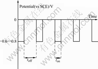
Fig.1 Schematic diagram of pulse potential used to deposit CIS films
The deposition time was 60 min. The as-deposited films were annealed at 450 �� for 30 min in flowing Ar. The crystalline properties, surface morphology and the chemical composition of the as-deposited and annealing-treated films were characterized by X-ray diffractometry (XRD, Rigaku3014), scanning electron microscopy (SEM, JSM-6360LV) and energy dispersive X-ray spectroscopy (EDS, EDAX-GENSI-S60S), respectively.
3 Results and discussion
3.1 Electrochemical analysis
The electrodeposition of CIS film on cathode is most likely caused by the combination of electrochemical and chemical reactions as follows:
Cu2++2e��Cu E0=0.342 V (vs NHE) (1)
In3++3e��In E0=-0.338 V (vs NHE ) (2)
H2SeO3+4H++4e��Se +3H2O E0=0.74 V (vs NHE ) (3)
Cu, In, Se��CuaInbSec (4)
Linear potential scan (Fig.2) was conducted by EG&G PAR 273A to estimate the reduction potential of each element. The optimum potentials for reduction of Cu2+/Cu, SeO32-/Se, In3+/In elements are -0.38, -0.47 and -0.55 V (vs SCE), respectively. As the potential moves to more negative value than -0.75 V (vs SCE), hydrogen bubble generates. The polarization of these reduction potential to the theoretically expected values is caused by various factors, such as the constituents and concentration of the electrolyte, pH, substrate, the absence or presence of stirring, complexing agents[13-14]. From the curve, the suitable potential range for co-deposition is found to be from -0.55 to -0.75 V (vs SCE).
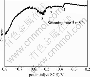
Fig.2 I��V curve of linear potential scan
The theoretical thickness of the electrodeposited CuInSe2 thin films is determined by Faraday��s law as following relationship:
 (5)
(5)
where n is the number of electrons transferred, F is Faraday��s number, A is the electrode area, i is the current delivered, t is the deposition time, m is the relative molecular mass (366.28 g/mol) and �� is the density of the electrodeposited CIS film(5.77 g/cm3). The number of electrons transferred is taken as 13, if the total electrode reaction is assumed to occur:
Cu2++ In3++ 2H2SeO3 + 8H++13e��CuInSe2+6H2O (6)
In this work, the value of i��t is obtained from Fig.1, and the n-value is determined as 13.4[6]. On the basis of the theoretical calculation using Enq.(5), the deposited thickness of the CIS material is controlled in the range between 0.8 and 1.5 ��m. Since the as-deposited films are not compact, we consider that the theoretical thickness is close to that of the films annealed[15].
3.2 Annealing
Fig.3 shows typical XRD patterns of as-deposited and annealed CIS films with a pulse potential of -0.70 V (vs SCE), duty cycle of 33% and pulse period of 3 ms. The pattern of the as-deposited film shows only weak and board peaks (Fig.3(a)), which means the crystallinity is very poor, and the CIS compound is not formed. As shown in Fig.3(b), the ternary compound CuInSe2 is formed. Furthermore, the crystallinity is improved by annealing, showing the sharp and intense diffraction peaks of the (112), (220, 204) and (312, 116). The chalcopyrite structure is also confirmed by preferred orientation to (101), (103) and (211).
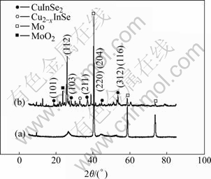
Fig.3 XRD patterns of electrodeposited CIS films: (a) As-deposited; (b) Annealed
Fig.4 shows the surface morphologies of the electrodeposited samples before and after annealing. The as-deposited film is stacked by many small particles that have well-defined boundaries. After annealing, boundaries fuse to be irregular because of interdiffusion and selenization reaction, and the particles grow to larger grains resulted from recrystallization.
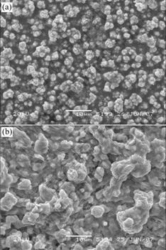
Fig.4 Morphologies of electrodeposited CIS thin films before and after annealing: (a) Before annealing; (b) After annealing
3.3 Pulse parameters
The surface morphologies of electrodeposited films with various duty cycle �� at pulse potential of -0.70 V (vs SCE) and pulse period of 3 ms are shown in Fig.5. There are some change with various ��. The surface is comparably rough for ��=10%. The film deposited with ��=33% has the most homogenous and smoothest surface. As the duty cycle increases, the surface becomes more rough and shows a dendrite structure. CIS is deposited onto the cathode plate when the current is negative during ton. On the other hand, the projecting parts of deposited CIS surface selectively dissolve back to the aqueous solution when the current is positive during toff. The surface smoothing lies on the balance between deposition during ton and dissolution during toff in electrode surface[10]. For �� smaller than 33%, a comparably longer duration of dissolving leads to rather rough surfaces. In contrast, the selective dissolution of projecting parts from the surface is not sufficient for �� larger than 33%.
Fig.5 Morphologies of electrodeposited films with various duty cycle ��: (a) ��=10%; (b) ��=33%; (c) ��=50%; (d) ��=75%; (e) ��=100%
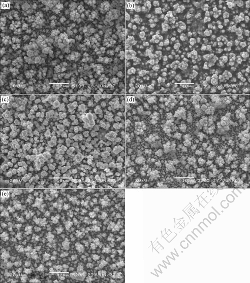
Fig.6 shows the Cu/In and Se/(Cu+In) ratios analyzed by EDS of electrodeposited films at various duty cycle ��. The influence disciplinarian of duty cycle on Cu/In ratio is not obvious. The Se/(Cu+In) ratio decreases as duty cycle �� increases and shows Se-rich, and Se concentration would be changed largely after annealing.
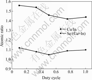
Fig.6 Molar ratio of electrodeposited films with various duty cycle ��
So, it can be confirmed that the duty cycle of ��=33% is the most suitable condition for electrodeposition of CIS precursor film from this experiment.
In addition, the influence of pulse period T (1 ms, 3 ms, 6 ms and 9 ms) on electrodeposited film quality was investigated. There are no remarkable differences observed among these surface morphologies and compositions. This means that the best pulse period T cannot be confirmed from these SEM and EDS results which are not listed here.
Fig.7 shows XRD patterns of annealed films electrodeposited under various pulse potentials ranging from -0.6 to -0.8 V (vs SCE) with a pulse period of 3 ms and a duty cycle of 33%. There are no remarkable differences observed among these XRD patterns. Every diffraction pattern shows the (112) and other diffraction characteristic of CuInSe2 chalcopyrite structure. This indicates that chalcopyrite phase CuInSe2 thin films can be achieved under a wide pulse potential range.
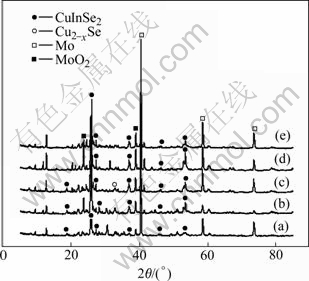
Fig.7 XRD patterns of CIS films electrodeposited and annealed at different pulse potential: (a) -0.6 V; (b) -0.65 V; (c) -0.7 V; (d) -0.75 V; (e) -0.8 V (vs SCE)
Fig.8 shows the Cu/In and Se/(Cu+In) molar ratios analyzed by EDS of these annealed films as function of pulse potential. The molar ratios of Cu/In and Se/(Cu+ In) indicate the stoichiometric state of pulsed-plating electrodeposited films. In addition, as the pulse potential moves to negative values, the molar ratios of Cu/In and Se/(Cu+In) increase. This may be attributed to the fact that the increment of Cu and Se deposition rate is larger than that of In and (Cu+In) deposition rate, as pulse potential moves to negative. All samples are Cu-rich in composition. The molar ratio of Cu/In��1, is maintained with wide pulse potentials ranging from -0.6 to -0.75 V (vs SCE), and the sample with pulse potential of -0.65 V (vs SCE) is the proximal stoichiometric one.
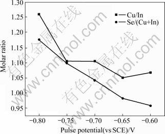
Fig.8 Molar ratio of films electrodeposited and annealed as function of pulse potential
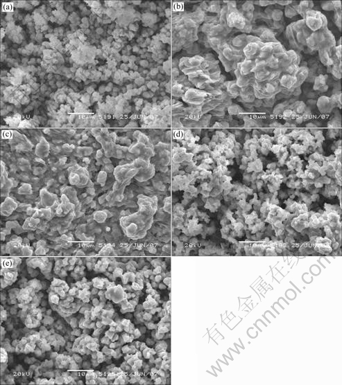
The surface morphologies of these electrodeposited and annealed CIS thin films with various pulse potentials ranging from -0.6 to -0.8 V (vs SCE) are shown in Fig.9. Irrespective of the deposition potential, the surface morphology reveals a dendrite structure, due to the limited ion concentration, which is influenced by the electrolyte concentration and duration of deposition. Remarkable changes are observed as the pulse potential varies. It is found that films with good morphology and large grain size can be obtained with pulse potentials from -0.65 to -0.70 V (vs SCE). The uniformity of film at a pulse potential fo -0.6 V (vs SCE) is worse than that at a pulse potential from -0.65 to -0.70 V (vs SCE). This is maybe because the number of nucleation sites in the case of a pulse potential -0.6 V (vs SCE) is fewer than that in the case of a pulse potential of from -0.65 to -0.70 V (vs SCE), and consequently, the coalescence of the elements occurs in fewer nucleated sites. On the other hand, when the applied pulse potential is more negative than -0.70 V (vs SCE), particles separating from solution do not have enough time to diffuse to the proper sites of the small grains formed previously on electrode surface at the high deposition rate, and hydrogen generates obviously, so the film surface morphologies become worse during depositing process and these films are not fit for application.
Fig.9 Morphologies of electrodeposited CIS thin films with various pulse potentials: (a) -0.6 V; (b) -0.65 V; (c) -0.7 V; (d) -0.75 V; (e) -0.8 V (vs SCE)
4 Conclusions
CuInSe2 thin films with chalcopyrite structure were prepared by pulse-plating electrodeposition and post-annealing treatment. From the linear potential scanning curve, the suitable potential range for co-deposition was found to be from -0.55 to -0.75 V (vs SCE). The as-deposited film had poor crystallinity, and the annealed sample showed improved crystallinity and chalcopyrite structure. Films with good morphology, large grain size and stoichiometric composition could be obtained on the most suitable conditions as pulse potential ranging from -0.65 to -0.70 V (vs SCE), a pulse period of 1-9 ms and a duty cycle of 33%.
References
[1] ROCKETT A, ABOUELFOTOUH F, ALBIN D, BODE M, ERMER J, KLENK R, LOMMASSON T, RUSSELL T W F, TOMLINSON R D, TUTTLE J, STOLT L, WALTER T, PETERSON T M. Structure and chemistry of CuInSe2 for solar cell technology: Current understanding and recommendations [J]. Thin Solid Films, 1994, 237: 1-11.
[2] CONTRERAS M A, TUTTLE J, GABOR A, TENNANT A, RAMANATHAN K, ASHER S, FRANZ A, KEANE J, WANG L, SCOFIELD J, NOUFI R. High efficiency Cu(In,Ga)Se2-based solar cells: Processing of novel absorber structures [C]// 1st World Conf Photovoltaic Energy Conversion. Piscataway, NJ, USA: IEEE, 1994: 68-75.
[3] CONTRERAS M, RAMANATHAN K, ABUSHAMA J, HASOON F, YOUNG D, EGAAS B, NOUFI R. Diode characteristics in state-of-the-art ZnO/CdS/Cu (In1-xGax)Se2 solar cells [J]. Prog Photovolt: Res Appl, 2005, 13: 209-216.
[4] BHATTACHARYA R N, FERNANDEZ A M. CuIn1-xGaxSe2-based photovoltaic cells from electrodeposited precursor films [J]. Solar Energy Materials and Solar Cells, 2003, 76: 331-337.
[5] LINCOT D, GUILLEMOLESA J F, TAUNIER S, GUIMARD D, SICX-KURDI J, CHAUMONT A, ROUSSEL O, RAMDANI O, HUBERT C, FAUVARQUE J P, BODEREAU N, PARISSI L, PANHELEUX P, FANOUILLERE P, NAGHAVI N, GRAND P P, BENFARAH M, MOGENSEN P, KERREC O. Chalcopyrite thin film solar cells by electrodeposition [J]. Solar Energy, 2004, 77: 725-737.
[6] THOUIN L, VEDEL J. Electrodeposition and characterization of culnSe2 thin films [J]. J Electrochem Soc, 1995, 142(9): 2996-3001.
[7] UGARTE R,SCHREBLER R,CORDOVA R,DALCHIELE E A,GOMEZ H. Electro-deposition of CuInSe2 thin flms in a glycine acid medium [J]. Thin Solid Films, 1999, 340: 117-124.
[8] EDAMURA T, MUTO J. Preparation and characterization of pulse-plating electrodeposited CuInSe2 thin films [J]. Journal of Materials Science: Materials in Electronics, 1994, 5: 275-279
[9] ENDO S, NAGAHORI Y, NOMURA S. Preparation of CuInSe2 thin films by the pulse-plated electrodeposition [J]. Jpn J Appl Phys, 1996, 85: 1101-1103.
[10] NOMURAS, NISHIYAMAK, TANAKAK, SAKAKIBARAM, OHTSUBOM, FURUTANIN, ENDOS. Preparation of cuInSe2 thin films on Mo-coated glass substrates by pulse-plated electrodeposition [J]. Jpn J Appl Phys, 1998, 37: 3232-3237.
[11] PROSINI P P, ADDONIZIO M L, ANTONAIA A. Effect of substrate surface treatment on the nucleation and crystal growth of electrodeposited copper and copper-indium alloys [J]. Thin Solid Films, 1997, 298: 191-196.
[12] BERTTAIN W H, BOODY P J. The interface between germanium and a purified neutral electrolyte [J]. Electrochem J Soc, 1962, 107: 574-582.
[13] PAUNOVIC M, SCHLESINGER M. Fundamentals of electrochemical deposition [M]. New Jersey: Wiley�CInterscience, 1998: 167-171.
[14] KANG S H, KIM Y K, CHOI D S, SUNG Y E. Characterization of electrodeposited CuInSe2 (CIS) film [J]. Electrochimica Acta, 2006, 51: 4433-4438.
[15] ZHANG L, JIANG F D, FENG J Y. Formation of CuInSe2 and Cu(In,Ga)Se2 films by electrodeposition and vacuum annealing treatment [J]. Solar Energy Materials and Solar Cells, 2003, 80: 483-490.
Foundation item: Project(06FJ4059) supported by Hunan Provincial Academician Foundation
Corresponding author: LIU Fang-yang; Tel: +731-8830474; E-mail: liufangyang1984@126.com
(Edited by YUAN Sai-qian)