Trans. Nonferrous Met. Soc. China 23(2013) 433-438
Temperature coefficient of resistivity of TiAlN films deposited by radio frequency magnetron sputtering
Min-Ho PARK, Sang-Ho KIM
School of Energy, Materials and Chemical Engineering, Korea University of Technology and Education, 1600 Chungjeol-ro, Byungcheon-myun, Dongnam-gu, Cheonan, Chungnam 330-708, Korea
Received 2 May 2012; accepted 25 September 2012
Abstract: Titanium aluminum nitride (TiAlN) film, as a possible substitute for the conventional tantalum nitride (TaN) or tantalum-aluminum (TaAl) heater resistor in inkjet printheads, was deposited on a Si(100) substrate at 400 ��C by radio frequency (RF) magnetron co-sputtering using titanium nitride (TiN) and aluminum nitride (AlN) as ceramic targets. The temperature coefficient of resistivity (TCR) and oxidation resistance, which are the most important properties of a heat resistor, were studied depending on the plasma power density applied during sputtering. With the increasing plasma power density, the crystallinity, grain size and surface roughness of the applied film increased, resulting in less grain boundaries with large grains. The Ti, Al and N binding energies obtained from X-ray photoelectron spectroscopy analysis disclosed the nitrogen deficit in the TiAlN stoichiometry that makes the films more electrically resistive. The highest oxidation resistance and the lowest TCR of -765.43��10-6 K-1 were obtained by applying the highest plasma power density.
Key words: inkjet printhead; TiAlN; radio frequency magnetron sputtering; temperature coefficient of resistivity
1 Introduction
The thermal inkjet printer has emerged as one of the mainstream digital printing technologies because it is relatively less expensive to manufacture and is easily adaptable to color printing applications [1].
Inkjet technologies are usually divided into continuous and drop-on-demand (DOD) printing methods. The DOD inkjet printhead is used most widely for small office and home applications, although it may be used in various other fields. Among the several actuating methods, the thermal inkjet printing method is the most successful due to its low cost and high printing quality [2].
In the thermal inkjet printer, generally, a thin-film heater resistor that converts electrical energy into thermal energy is used to eject the ink. Because the film is subjected to severe environments, such as high operating temperature, chemical attack by the ink, and mechanical stresses arising from cavitation forces during the printing operation, it must be environmentally stable [1]. In addition, the heater resistor material should have a low temperature coefficient of resistance (TCR) to produce stable ejection of ink and a strong resistance against both corrosion and oxidation to prevent becoming degraded during use [3].
The TCR value of typical TaN0.8 is known as 336��10-6 K-1 [4]. Titanium aluminum nitride (TiAlN) film has many attractive properties for use as a heater resistor, such as an appropriate resistivity range with sufficiently low TCR and high oxidation resistance at high temperatures.
In this study, the TiAlN thin films were deposited by RF magnetron sputtering on Si(100) substrate at several different plasma power densities. The TCR and oxidation resistance of the TiAlN thin films were evaluated depending on the plasma power density that produced them, and discussed in relationship with their micro morphology and chemical bonding state.
2 Experimental
The substrate used in this study was p-type Si(100) wafers. The substrate was chemically cleaned within an ultrasonic wave bath with acetone, ethanol and deionized water to remove the surface organic contaminants. The TiAlN films were grown by the radio frequency (RF) magnetron co-sputtering from AlN and TiN ceramic targets (RND Korea). Figure 1 shows a schematic diagram of the RF magnetron sputtering.

Fig. 1 Schematic diagram of RF magnetron sputtering
On the AlN target, the plasma power density was varied from 10.85 to 19.74 W/cm2; on the TiN target, the plasma power density was varied from 5.92 to 11.84 W/cm2 to make the mole ratio of Al to Ti in the TiAlN films near 1:1. Figure 2 illustrates the mole ratio of Al to Ti vs the plasma power density changed.

Fig. 2 Mole ratio of Al to Ti in TiAlN films vs plasma power density
The plasma power densities at the AlN target were 10.85, 11.84, 14.80 and 19.74 W/cm2 and at the TiN target, the densities were 5.92, 7.89, 9.87 and 11.84 W/cm2, respectively, measured by the energy dispersive spectroscopy of the field emission scanning electron microscopy (FESEM, JEOL JEM-7500F). Other deposition parameters were kept constant, as listed in Table 1.
The film thickness was measured with a surface profilometer (TENCOR-2) and kept near 2000  for all samples by adjusting the deposition time. The crystallinity and orientation of the grain growth of the TiAlN films were characterized using an X-ray diffractometer (XRD, Rigaku RTP 200 RC) with Cu K�� radiation over the 2�� range of 20��-70��; the morphology of the films was observed using the FE-SEM. The Ti-Al-N bonding state was investigated by X-ray photoelectron spectroscopy (XPS, SIGMA PROBE) using mono-chromatic Al K�� radiation, a hemispherical electrostatic analyzer and a position-sensitive multichannel plate detector. The energy scale of the XPS spectrometer was calibrated by employing the C 1s peak at 284.6 eV. The surface roughness was examined using an atomic force microscope (AFM, SOLVER P47-PRO). The sheet resistance of the films was measured using a four-point probe (Guardian Scientific 402S), and the TCR values were measured with a digital multimeter (HP3457A) while heating the films from 30 ��C to 170 ��C in a thermostatically-controlled oven.
3 Results and discussion
TiAlN has either a B1-NaCl or a wurtzite lattice structure, depending on the Al to Ti mole ratio, as shown in Fig. 3. In Fig. 3(a), the large circles are the locations of Ti or Al atoms and the small circles are the locations of N atoms. Since the atomic radius of Al is smaller than the atomic radius of Ti, when the Al atoms substitute for up to 60% of the Ti atoms, the B1-NaCl structure remains but lattice parameter a decreases. However, when the Al content exceeds 70%, the lattice structure transforms to the wurtzite structure as shown in Fig. 3(b) [5]. In this study, since the Al to Ti mole ratio remains in the range of 47%-51%, all TiAlN films would have a B1-NaCl lattice structure.
Table 1 Deposition parameters for RF sputtering of TiAlN film


Fig. 3 Lattice structure of TiAlN

Fig. 4 XRD patterns of TiAlN films deposited with various plasma power densities
Figure 4 shows the X-ray diffraction patterns of the TiAlN films deposited with different plasma power densities. At a low power density, the film was nearly amorphous, but as the power density increased beyond medium, the diffraction peaks corresponding to TiAlN (200) and (220) appeared and the intensity increased. This indicates that increasing the plasma power density produces the formation of a better crystalline film. It is generally understood that a higher energy of adsorbed atoms on the substrate makes the atoms crystallize when the highly dense plasma power is applied [6].
Figure 5 represents the surface morphologies of TiAlN films with different plasma power densities, confirming that the grain size increases as the power density is increased to medium high, and above that point, it decreases slightly. The energy and number of ad-atoms become large as plasma power density grows, so the grain size expands before it is hindered at a very high plasma power density by adjacent ad-atom competitors. In other words, the trade-off effect of ad-atom energy and numbers, depending on the plasma power density, establishes the maximum grain size at the medium power level.
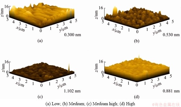
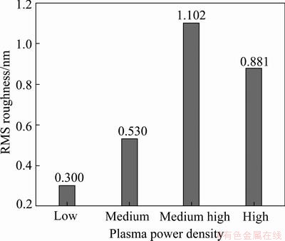
Figure 6 shows the 3D AFM morphologies and Fig. 7 shows the root mean square (RMS) of the surface roughness on TiAlN films. In a manner similar to the previous variation of grain size, the RMS surface roughness was largest (1.102 nm) at the medium high power density, and then at higher plasma power density, the RMS surface roughness decreased slightly again, validating the mechanism in variation of grain size.

Fig. 5 Surface morphologies of TiAlN films deposited with various plasma power densities

Fig. 6 3D AFM morphologies of TiAlN films with various plasma power densities

Fig. 7 Evolution of surface roughness of TiAlN films deposited with various plasma power densities
The peak position and relative intensity of the XPS can be used to identify the chemical bonding states of elements in the thin films. Figure 8 illustrates the XPS core level spectra of each element in TiAlN films. The Ti 2p spectrum shown in Fig. 8(a) has clearly resolved into three doublet peaks, which correspond to the Ti 2p3/2 core level at low binding energy ranging from 454 to 460 eV. In this range, the low binding energy (~455.8 eV) is attributed to Ti��N (TiN) bonds, the medium binding energy (~457.0 eV) is related to the Ti��N��O (TiNxOy) bonds and the high binding energy (~458.3 eV) could be assigned to the Ti��O (TiO2) bonds [7-9].
When the power density was at the medium high and high levels, the peaks�� relative shoulder intensities located at 457.0 eV and 458.3 eV are high in comparison with the peak intensity at 455.8 eV, signifying a greater binding energy of Ti 2p3/2 electrons. This implies a weaker binding effect of coupling N atoms to Ti atoms, while the Al 2p binding energy moves to the lower binding energy side, as seen in Fig. 8(b), when the plasma power density increases to medium high or high state. This indicates that more N atoms were coupled to Al atoms at the high power density, making the electrons in the Al 2p orbits easy to detach with less energy to the vacuum level [10-12].

Fig. 8 XPS core level spectra of TiAlN films deposited with various plasma power densities
The N 1s spectra (Fig. 8(c)) produced with higher plasma density reveal the locations near the N-Ti and N-Al binding energies, which are centered at 396.7 and 396.8 eV, respectively, as reported by BERTOTI [13]. N atoms in TiAlN films are thought to exist inside the effective binding range of Ti or Al atoms in the B1-NaCl lattice, as shown in Fig. 3. From these XPS analyses, we know that there are an insufficient number of nitrogen atoms available because at the high plasma power density, they concentrate onto the more attractive Al atoms with their smaller atomic radii.
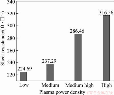
Figure 9 demonstrates that the sheet resistance changes monotonically with the plasma power density. This seems due to the depletion of nitrogen at the high plasma power density, as discussed in the previous paragraph. Generally, large grains provide a lower sheet resistance in film, although in this case the large grain effect at the high plasma power density is likely small enough to be offset by the nitrogen deficit effect. The sheet resistance of TiAlN is in the range of 225-317 ��/��, suggesting the formation of a conductive ceramic compound because AlN and TiN films yield a sheet resistance of about 1022 ��/�� [14] and 1 ��/��, respectively. Our results are also comparable to the 141-1396 ��/�� range of the TaN0.8 available commercially [15].

Fig. 9 Sheet resistance of TiAlN films deposited with various plasma power densities
The TCR characteristics of TiAlN films are shown in Fig. 10. The TCR value was calculated using the following formula: TCR=(R170�CR30)/[R30(170-30)]��106, where Rx is the resistivity at temperature x. The TCR value decreases with increasing plasma power density and is lowest (-765.43��10-6 K-1) when the plasma power density is high.

Fig. 10 TCR value of TiAlN films deposited with various plasma power densities
The relationship of lower TCR with higher plasma power density comes from the higher sheet resistance persisting within a relevant range for use as a heat resistor. Oxidation resistance measured from the variation of sheet resistance after maintaining at 500 and 600 ��C for 30 min is shown in Fig. 11. In a manner similar to TCR, oxidation resistance is better at the high plasma power density. This oxidation resistance also should be due to the higher sheet resistance and the sound crystallinity of TiAlN films with larger grains obtained at the high plasma power density.

Fig. 11 Variation of sheet resistance of TiAlN films deposited with various plasma power densities
4 Conclusions
TiAlN films were prepared by RF magnetron sputtering at several different plasma power densities. Lower TCR and higher oxidation resistance were obtained with films sputtered at the high power density. These results are attributable to a desirably-high sheet resistance resulting from the N deficit in TiAlN films at the high power density and the compensation obtained with better crystallinity and large grains. Also, TiAlN films produced with the high plasma power density showed better oxidation resistance, which can be ascribed to the higher sheet resistance and sound crystallinity with larger grains.
References
[1] ADEN J S,  J H, COLLINS V, CROOK M D,
  A, HESS U E. The third-generation hp thermal inkjet printhead [J]. Hewlett-Packard Journal, 1994: 41-45.
[2] LIM J H, KUK K, SHIN S J, BAEK S S, KIM Y J, SHIN J W, OH Y S. Failure mechanisms in thermal inkjet printhead analyzed by experiments and numerical simulation [J]. Microelectronics Reliability, 2005, 45: 473-478.
[3] KWACK W S, MOON H S, JEONG S J, WANG Q M, KWON S H. Hybrid functional IrO2-TiO2 thin film resistor prepared by atomic layer deposition for thermal inkjet printheads [J]. Transactions of Nonferrous Metals Society of China, 2011, 21(s1): s88-s91.
[4] KWON S H, KANG S W, KIM K H. Controlling the temperature coefficient of resistance and resistivity in RuO2�CTiO2 thin films by the intermixing ratios between RuO2 and TiO2 [J]. Applied Physics Letters, 2008, 92: 181903.
[5] KIMURA A, KAWATE M, HASEGAWA H, SUZUKI T. Anisotropic lattice expansion and shrinkage of hexagonal TiAlN and CrAlN films [J]. Surface & Coatings Technology, 2003, 169-170: 367-370.
[6] PAN Huai-jian, YANG Yong. Effects of radio-frequency sputtering powers on the microstructures and electrochemical properties of LiCoO2 thin film electrodes [J]. Journal of Power Sources, 2009, 189: 633-637.
[7]  J, KARLSSON L, BRAUN S, MURDEY R,
  A, HULTMAN L. Structure and mechanical properties of arc evaporated Ti�CAl�CO�CN thin films [J]. Surface & Coatings Technology, 2007, 201: 6392-6403.
[8] CHENG Y, ZHENG Y F. Surface characterization and mechanical property of TiN/Ti-coated NiTi alloy by PIIID [J]. Surface & Coatings Technology, 2007, 201: 6869-6873.
[9] BAKERA M A, GREAVESA S J, WENDLERB E, FOX V. A comparison of in situ polishing and ion beam sputtering as surface preparation methods for XPS analysis of PVD coatings [J]. Thin Solid Films, 2000, 377-378: 473-477.
[10] SCHOSER S, BRAUCHLE G, FORGET J, KOHLHOF K, WEBER T, VOIGT J, RAUSCHENBACH B. XPS investigation of AlN formation in aluminum alloys using plasma source ion implantation [J]. Surface & Coating Technology, 1998, 103-104: 222-226.
[11] MOULDER J F, WATSON D G, STICKLE W F. Factor analysis of angle-dependent XPS Si 2p spectra from dry processed Si wafers [J]. Journal of Electron Spectroscopy and Related Phenomena, 1990, 52: 303-309.
[12] MAHMOOD A, RAKOV N, XIAO M. Influence of deposition conditions on optical properties of aluminum nitride (AlN) thin films prepared by DC-reactive magnetron sputtering [J]. Materials Letter, 2003, 57: 1925-1933.
[13]  . Characterization of nitride coatings by XPS [J]. Surface & Coating Technology, 2002, 151-152: 194-203.
[14] AXELBAUM R L, LOTTES C R, HUERTAS J I, ROSEN L J. [C]//Symposium (International) on Combustion, 1996, 26: 1891-1897.
[15] KANG S M, YOON S G, SUH S J, YOON D H. Control of electrical resistivity of TaN thin films by reactive sputtering for embedded passive resistors [J]. Thin Solid Films, 2008, 516: 3568-3571.
��Ƶ�ſؽ������TiAlN��Ĥ�ĵ������¶�ϵ��
Min-Ho PARK, Sang-Ho KIM
School of Energy, Materials and Chemical Engineering, Korea University of Technology and Education, 1600 Chungjeol-ro, Byungcheon-myun, Dongnam-gu, Cheonan, Chungnam 330-708, Korea
ժ Ҫ��TiAlN��Ĥ��һ���п�����Ϊ��ī��ӡͷ�д�ͳ��TaN��TaAl���ȵ�������Ʒ������TiN��AlN���вģ���400 ��C������Ƶ�ſؽ��乲����������Si(100)�������Ʊ�TiAlN��Ĥ���о��˴ſؽ������ʱ�������幦���ܶȶ�TiAlN��Ĥ�������¶�ϵ���Ϳ��������ܵ�Ӱ�졣���������TiAlN��Ĥ�Ľᾧ�ȡ������ߴ�ͱ���ֲڶ����ŵ������幦���ܶȵ����Ӷ����Ӷ����´�����С���硣X���߹�����������õ���Ti�� Al ��N�ļ����ܱ�����TiAlN�е��ػ�ѧ����ѧ��ȱʹTiAlN��Ĥ�ĵ����������ߵ������幦���ܶ����Ʊ���TiAlN��Ĥ������ߵĿ��������ܺ���͵ĵ������¶�ϵ��(-765.43��10-6 K-1)��
�ؼ��ʣ���ī��ӡͷ��TiAlN����Ƶ�ſؽ��䣻�������¶�ϵ��
(Edited by Hua YANG)
Foundation item: Project (M-2009-01-0029) supported by Fundamental R&D Program for Core Technology of Materials, Korea
Corresponding author: Sang-Ho KIM; Tel: +82-41-560-1325; E-mail: shkim@koreatech.ac.kr
DOI: 10.1016/S1003-6326(13)62481-4