Trans. Nonferrous Met. Soc. China 22(2012) s825-s830
An effective round ball tool in electrochemistry process as novel reuse fabrication technology
P. S. PA
Department of Digital Content Design, Graduate School of Toy and Game Design, National Taipei University of Education, Taipei 106
Received 21 May 2012; accepted 22 September 2012
Abstract: A reuse fabrication module using micro electrochemistry (MECM) with a round-ball tool to remove the defective In2O3SnO2 thin film from the surfaces of digital paper display was presented. The etching effect improves that the number of the round-balls decreases for promoting the concentration of electric power and increasing discharge space. Using a small size of the round-ball tool takes less time for the same amount of In2O3SnO2 layer removal since the effect of MECM is easily developed for supplying of sufficient electrochemical power. A higher feed rate of the poly ethylene terephthalate (PET) diaphragm combines with enough electric power to drive fast etching rate. A pulsed direct current can improve the effect of dreg discharge and is advantageous to couple this current with the fast feed rate of the workpiece. Through the ultra-precise etching of In2O3SnO2, the optoelectronic semiconductor industry can effectively reuse the defective products, reducing production costs. This precision etching process is of high efficiency and requires only a short period of time to remove the In2O3SnO2 nanostructures.
Key words: thin film; round-ball tool; In2O3SnO2; micro electrochemistry; digital paper display
1 Introduction
The rewritable electronic paper display, also known as digital paper (e-paper), is an alternative and promising application of liquid crystal display (LCD) in informational media [1]. The basic construction of the touch-panel is similar to that of an LCD panel, with two substrate coatings of an indium tin oxide (In2O3SnO2) transparent conductive film. The sheet resistance of the In2O3SnO2 transparent conductive film used on the touch-panel is higher than the LCD panel [2]. The primary cause of decrease in yield rate of LCD production is dust. When dust particles become attached to the LCD substrate, they impair its function and cause breaks in the circuit, short-circuits or poor performance. Upon examination of LCD defects, it was found that many were dust-related [3,4].
Color filters are the critical components of LCDs, because each TFT (thin film transistor) array is matched to a color filter of the same size, which means that the quality of the color filter has a decisive effect on its color reproduction [5]. The electrochemical machining (ECM) is based on the electrochemical reaction between an electrode and a workpiece. The main difficulty lies in the design of tool electrodes due to the complicated process of metal removal. In addition, workpiece machining through the electrochemical process can improve the precision with the appropriate control of machining conditions or the electrode geometry [6,7].
The existing data show that the gap width between the electrode and workpiece directly influences the current condition and the discharge dreg of the electrolyte [8]. The experimental results of MILEHAM et al [9,10] proved that the quality of the machined surface would be influenced by factors including current density, flow rate of electrolyte and the gap width in the electrochemical machining. SHEN [11] used NaNO3 as the electrolyte that allows for the electropolishing on the die surface. Electropolishing is a surface finish process using PO4-3-P as the electrolyte for brass alloys and zinc alloys [12,13]. CAGNON et al [14] and KIM [15] showed that the machining resolution can be shortened to a few micrometers by applying ultra short pulses on the order of nanoseconds, and the microstructures can be machined by ECM.
In2O3SnO2 thin films are transparent and conductive and are deposited as a thin film on glass or polymer substrates by vacuum thermal evaporation, vacuum sputtering or e-beam sputtering used in optoelectronic devices produced semiconductor fabrication techniques. However, the low yield during production was easily observed [16,17]. The material cost of most panels of different sizes exceeds 50% of the total cost of the panels. Thus, in order to reduce the material cost, constructing a precision reclaim mechanism and executing an effective reclaim process are the most important issues in the semiconductor industry [18]. In addition, workpiece machining through the electrochemical process can improve efficiency with the appropriate control of the machining conditions or the electrode geometry. A plate-form electrode was developed as a design tool used in recycling systems, and good removal effects were obtained through the careful design of the experimental conditions [19]. In the current work, we conducted a new mechanism using micro electrochemistry (MECM) as a precision-reclaim process of In2O3SnO2 thin film coatings with a round-ball tool on the surface of the poly ethylene terephthalate (PET) diaphragm of digital paper. The adopted precision recycling process is low cost and highly efficient. The development of the proposed precision reclaim process design is based on technical and economical considerations.
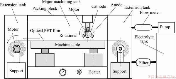
Fig. 1 Mechanism design and experimental setup of precision reuse process
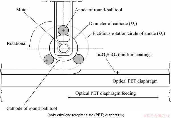
Fig. 2 Configuration of electrodes and workpieces
2 Experimental
The material of the workpiece uses an optical PET diaphragm of digital paper (400 mm in width; 0.2 mm in thickness). The workpiece was placed in the electrolytic tank and was soaked in the electrolyte to begin the recycling process. The equipment for the precision- reclaim process of the indium tin oxide (In2O3SnO2) thin film included automatic feeding devices, a DC power supply, a heater, a pump, a flow meter, an electrolytic tank and a filter. The mechanism and the experimental setup of the precision recycle process are illustrated in Fig. 1. The designed round-ball tool is shown in Fig. 2. The reduction in the removal from the surface of the optical PET diaphragm after micro electrochemistry (MECM) for the In2O3SnO2 thin film coatings is 20 nm. The electrolyte was NaNO3 of 10% and PO4-3-P 5% (mass fraction). The flow rate of electrolytes was 15, 20, 25 and 30 L/min. The experimental parameters were electrolyte temperature, concentrations of the electrolytes, current rating, pulsed period and feed rate of the workpiece (optical PET diaphragm). The temperatures of the electrolyte were 35, 45, 55, and 65 °C, respectively. The current ratings were 50, 100, 150, 200 A, respectively. The feed rate of workpiece (optical PET diaphragm) was ranged from 600 to 1200 mm/min. The rotational speeds of the round-ball tool were 100, 200, 300 and 400 r/min, respectively. The diameter of the fictitious rotation circle of the round-ball tool (Da) and the gap-width (u) between cathode and the workpiece were 45, 2; 47, 3; 49, 4 and 51, 5 mm, respectively. The pulse periods (on/off time) were 100 ms/100 ms, 100 ms/200 ms and 100 ms/300 ms, respectively. All workpieces were cleaned with water after the recycle process and then dried by air. These recycled In2O3SnO2 thin film coatings were measured at more than two locations by the NanoSpec Film Thickness Measurement System (Nanospec Film Analyzer 3000).
3 Results and discussion
3.1 Target of In2O3SnO2 thin film coatings removal
The engineering specifications allow for the removal of defective indium tin oxide (In2O3SnO2) thin film coatings and for the reinstatement of the defective PET diaphragm onto the production line. The precision-reclaim process of the optical PET diaphragm of digital paper is to be extended to all of the in-house fabrications of optical PET diaphragms of digital paper, and adopted into their total recovery systems. Cost reduction is the ultimate goal when establishing recovery systems. The total recovery of the entire system, which prevents re-pollution, is just as important as the function of repairing defective products.
3.2 Performance assessment on round-ball tool design
Figure 3 shows that under fixed electrolyte concentrations and temperatures, an adequate feed rate of the optical PET diaphragm combined with enough electric power will completely remove the In2O3SnO2 thin film coatings. At a constant current rating, the PET diaphragm has an optimal feed rate for the removal process. Fast feed reduces the power delivered to the unit area of the plane surface, while slow feed increases the power delivered. The former could not supply sufficient electrochemical power, while the latter increases the removal time and the cost. In order to reach the same etching of a 20 nm In2O3SnO2 thin film coating, the following combinations of parameter values are suggested: 50 A and 600 mm/min, 100 A and 800 mm/min, 150 A and 1000 mm/min, 200 A and 1200 mm/min.
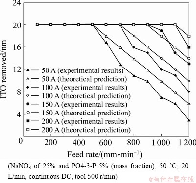
Fig. 3 Removal amount at different feed rates of poly ethylene terephthalate (PET) diaphragm using different current ratings
The formula on the theoretical removal rate on a purity metal derived from FARADAY’s Law is [6]
 (1)
(1)
where I is the current, t is time, F is the FARADAY constant, ni is the atom number, ai is the proportion of composition, and Mi is the atomic mass.
From Fig. 4, for an alloy consideration, let
 (2)
(2)
 (3)
(3)
where Ey is the removal rate in the longitudinal direction, A is the micro electrochemistry (MECM) area, ρ is the workpiece density, and f is the etching rate in the longitudinal direction. From the above equation, the theoretical feed rate of the workpiece for the same material etching rate can be calculated. Here, η, F, and A are regarded as constant for the material.
 (4)
(4)
where x is the gap between the electrode and the color filters, and h is the removal depth of the MECM (see Fig. 4).
 (5)
(5)
where L is the length from the center of the positive pole to the surface of the PET diaphragm, and Ra is the radius of fictitious rotation circle of the round-ball tool (see Fig. 4).
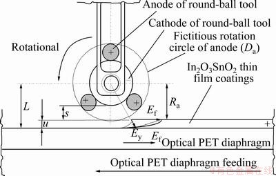
Fig. 4 Configuration of geometry of round-ball tool in MECM
 (6)
(6)
Squaring and simplifying Eqs. (5) and (6), we can obtain:
 (7)
(7)
where Ef is the feed velocity of the color filters. From Eq. (7),
 =
= (8)
(8)
where A is the micro electrochemistry (MECM) area, V is the voltage of the gap width, σ is the reciprocal resistance of the electrolyte. Using Eq. (8), the experimental results also agree well with the theoretical predictions (see Fig. 3). Compared with the experimental results, the removal depth u is directly proportional to the current rating I and is inversely proportional to the feed rate of the workpiece (Ef), which agrees well with the theoretical prediction (see Fig. 3).
The term “dregs” refers to the electrolytic product results from the machining gap in the process of micro electrochemistry. A better design process is useful for effective flushing, as the dregs are easy discharged out of the gap, which results in a better material removal effect [8,13]. Figure 5 illustrates that the small size of the round-ball (small diameter of the fictitious rotation circle of the round-ball tool), accompanied by the small gap-width between the cathode and the workpiece reduces the amount of time for effective micro electrochemistry (MECM) of In2O3SnO2 since the effect of the MECE is facilitated by supplying sufficient electrochemical power. Compared with the experimental results, the small gap-width accompanied by a large current rating and a fast feed rate of the workpiece, shows a reduction in the etching time. However, the dregs discharge from the small gap is difficult to processes. On the other hand, a small cathode (small diameter of the fictitious rotation circle of the round-ball tool) is accompanied by a large gap-width and results in a longer etch time since the MECM is limited. Compared with the experimental results and the Eq. (8), as far as the stable operation of MEC and dregs discharge is concerned (providing the reciprocal resistance of electrolyte (σ) stability), an appropriate diameter of the fictitious rotation circle of the round-ball tool of 49 mm, accompanied by the gap-width (3 mm) between the cathode and the workpiece is more effective in the current experiment.
Figure 6 shows the effects of the number of the round-balls. Decreasing the number of the round-balls not only reduces the resistance of dreg discharge and constructs a more effective flushing path along the features of the tool electrodes but also creates a more sufficient electrochemical power (higher current density) supplying. Meanwhile, the electrolytic products (dregs) and heat can be removed In2O3SnO2 more rapidly. Compared with the experimental results and the Eq. (8), adopting the number of the round-ball of one piece which is advantageous to In2O3SnO2 removal in the current work.
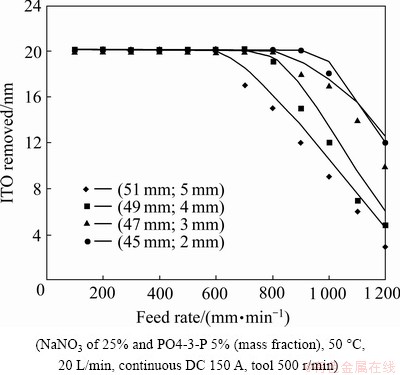
Fig. 5 Removal amount at different feed rates of poly ethylene terephthalate (PET) diaphragm using different diameters of fictitious rotation circle of round-ball tool and different gap widths
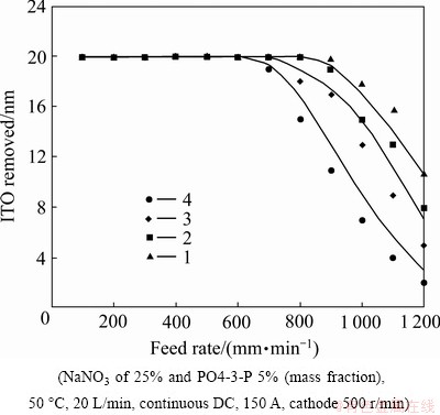
Fig. 6 Removal amounts at different feed rates of poly ethylene terephthalate (PET) diaphragm using different numbers of round-balls
Figure 7 illustrates different combinations of rotational speeds of the round-ball tool and flow rate of the electrolyte. From the experimental results, higher rotational speeds of the round-ball tool combines with higher flow rate of the electrolyte produced high rotational flow energy. The flow energy increases to elevate the discharge mobility in easily discharge the electrolytic depositions and in advantageous more heat to bringing away from the gap-width between the round-ball tool and the workpiece surface (optical PET diaphragm). It is believed that the combination of rotational speeds of the round-ball tool and flow rate of the electrolyte is desirable when associated with the fast feed rate of the optical PET diaphragm and improves the etching effect.
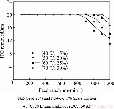
Fig. 7 Removal amount at different feed rates of poly ethylene terephthalate (PET) diaphragm using different rotational speeds of electrodes
From Fig. 7, compared with the experimental results and the Eq. (8), it can be seen that stably controlling the reciprocal resistance (σ) can stabilize the etching effect, and as a result, increase discharge mobility (providing a large round-ball tool rotational and providing a higher flow rate of the electrolyte), guide discharge transport, and provide flushing passage to provide the reciprocal resistance (σ) stability. Figure 8 shows the effects of the pulsed direct current. In order to reach the same removal amount of 20 nm for the In2O3SnO2 thin film coatings compared with the continuous direct current, the current rating needs to proportionally increase to compensate for the off-time. It is thought that the dreg discharge in MECM during the off-time is more complete, and that it can be beneficial when associated with the fast speed rate of the optical PET diaphragm.
 (9)
(9)
From Eq. (9), the response of the electrochemical etching only exists on the on-time period (TN). The off-time period (TF) provided the opportunity to proceed the dregs discharge of electrochemical etching. From Eq. (9), the removal depth (u) is directly proportional to the current rating (I) and is the inversely proportional to the feed rate of the workpiece (Ef), thus the current rating needs to be proportionally increased to reach the same etching amount compared with the continuous direct current.
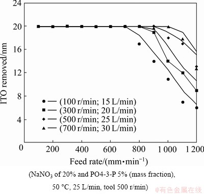
Fig. 8 Removal amount at different feed rates of poly ethylene terephthalate (PET) diaphragm using continuous and pulsed direct current
4 Conclusions
1) In2O3SnO2 can be removed completely by an adequate combination of optical PET diaphragm feed rate and electric power. For the etching process, a high flow velocity of the electrolyte provides larger discharge mobility and a better etching effect. A higher tool rotational speed corresponds to a higher etching rate for the In2O3SnO2. A higher current rating with a quicker optical PET diaphragm feed rate effectively achieves fast promotion of the removal effect.
2) A pulsed direct current can improve the effect of dreg discharge and is advantageous to couple this current with the fast feed rate of the workpiece. This improvement is associated with an increase in current rating. Decreasing the number of the round-balls or using a small size of the round-ball tool accompanied with a small gap-width between the cathode and the anode workpiece (In2O3SnO2) takes less time for the same amount of In2O3SnO2 thin film removal.
References
[1] Cueff r, Baud g, Benmalek m, Besse j p. Characterization and adhesion study of thin alumina coatings sputtered on PET [J]. Appl Sur Sci, 1997, 115: 292-298.
[2] Lai c c, Tsai c c, Neural c, Kalman f. Position estimation for touch panels [C]// Proceedings of the 2004 IEEE International Conference on Control Applications, 2004, 2: 1491-1496.
[3] Zhang y, Zhang j a. fuzzy neural network approach for quantitative evaluation of Mura in TFT-LCD [C]// Neural Networks and Brain 2005 ICNN&B ’05, 2005, 1: 424-427.
[4] Daeil k, Steven k. Effect of secondary ion beam energy and oxygen partial pressure on the structural, morphological and optical properties of ITO films prepared by DMIBD technique [J]. Int J of Surface and Coatings Technology, 2002, 154(2-3): 204-208.
[5] Lee p m, Chen h y. Adjustable gamma correction circuit for TFT-LCD [C]// IEEE Conference Proceeding, 2005, 1: 780-783.
[6] McGeough J A. Principles of electrochemical machining [M]. London: Chapman & Hall, 1974: 1-10.
[7] Jain V K, Nanda V N. Analysis of taper produced in size zone during ECD [J]. Precision Engineering, 1986, 8: 27-33.
[8] Datta M, Landolt D. Electrochemical machining under pulsed current conditions [J]. Elector Acta, 1981, 26: 899-907.
[9] Mileham A R, Harrey S J, Stout K J. The characterization of electrochemically machined surfaces [J]. Wear, 1986, 109: 207-214.
[10] Bejar M A, GUTIERREZ F. On the determination of current efficiency in electrochemical machining with a variable gap [J]. J Mat Proc Tech, 1983, 37: 691-699.
[11] Shen W F. The study of polishing of electric discharge-machined mold with ECM [D]. National Yunlin Institute of Technology, China, 1995.
[12] ISKANDER S S, Mansour I A S, SEDAHMED G H. Electropolishing of brass alloys in phosphoric acid [J]. Surface Technology, 1980, 10(5): 357-361.
[13] PA P S. Effective form design of electrode in electrochemical smoothing of end turning surface [J]. Journal of Materials Processing Technology, 2008, 195(1-3): 44-52.
[14] Cagnon L, Kirchner V, Kock M, Schuster R, Ertl G, Gmelin W T, Kuck H. Electrochemical miromachining of stainless steel by ultra short voltage pulses [J]. Z Phys Chem, 2003, 217: 299-313.
[15] Kim B H, Ryu S H, Choi S H, Chu C N. Micro electrochemical milling [J]. Journal of Micromechanics and Microengineering, 2005, 15: 124-129.
[16] Bender M, Seelig W, Daube C, Frankenberger C H, Ocker B. Dependence of film composition and thicknesses on optical and electrical properties of ITO-metal-ITO multilayers [J]. J Thin Solid Films, 1998, 326: 67-71.
[17] Besbes S, Ouada H B, Davenas J, Ponsonnet L, Jaffrezic N A. Effect of surface treatment and functionalization on the ITO properties for OLEDs [J]. Materials Science and Engineering, 26(2-3): 505-510.
[18] Tsai D M, Lin P C, Lu C J. An independent component analysis-based filter design for defect detection in low-contrast surface images [J]. Pattern Recognition, 2006, 39(9): 1679-1694.
[19] Pa P S. Precision removal of ITO layer using plate-form tool design [J]. J Solid State Electrochem, 2008, 12: 1445-1451.
(Edited by DENG Lü-xiang)
Foundation item: Project (100-2221-E-152-003) supported by National Science Council
Corresponding author: P. S. PA; Tel: +886-2-27321104; E-mail: myhow@seed.net.tw
DOI: 10.1016/S1003-6326(12)61811-1