文章编号: 1004-0609(2005)01-0100-05
热处理对(Mo0.85Nb0.15)Si2单晶显微结构的影响
杨海波, 李 伟, 单爱党, 吴建生
(上海交通大学 材料科学与工程学院, 上海 200030)
摘 要: 电弧熔炼制备的(Mo0.85Nb0.15)Si2合金为MoSi2(C11b结构)和NbSi2(C40结构)两相组织。 以电弧熔炼得到的合金为母合金, 通过光学悬浮区域熔炼法, 选择适当的生长速度4mm/h制备了(Mo0.85Nb0.15)Si2单晶, 单晶结构为C40结构。 对单晶在1200~1700℃进行不同时间的退火处理。 研究了不同热处理制度对合金显微结构的影响规律。 结果表明: 经1600℃, 6h退火处理后, 在合金中形成了排列紧密、 方向取向相同的全片层状结构, 片层间距为200~300nm。 经EDS分析, 这种片层结构由贫Nb的C11b相和富Nb的C40相组成。
关键词: Mo-Si系; 单晶; 金属间化合物; 退火; 显微结构 中图分类号: TG146.412
文献标识码: A
Effect of heat treatment on microstructure of (Mo0.85Nb0.15)Si2 single crystal
YANG Hai-bo, LI Wei, SHAN Ai-dang, WU Jian-sheng
(School of Materials Science and Engineering,
Shanghai Jiaotong University, Shanghai 200030, China)
Abstract: The intermetallics of (Mo0.85Nb0.15)Si2 with duplex C11b and C40 phases was prepared by arc-melting as the alloy used for single crystal growth. (Mo0.85Nb0.15)Si2 single crystal was then prepared by using optical floating zone melting method at a rate of 4mm/h. The crystal structure of the single crystal is C40 structure. A series of heat treatments (the treatment temperature is between 1200-1700℃) were conducted on the single crystal. The effect of heat treatment on microstructure was investigated in detail. A full lamellar structure was observed after annealing at 1600℃ for 6h, and the lamellar spacing is between 200-300nm. EDS analysis indicates that the lamellar structure consists of C11b phase (low Nb) and C40 phase (high Nb).
Key words: Mo-Si system; single crystal; intermetallics; annealing; microstructure
过去的十几年中, 硅化物基合金作为超高温结构材料的研究已经成为国内外研究工作者的研究重点之一[1-4]。 其中C11b结构的MoSi2具有优异的抗高温氧化性能及潜在的低温塑性变形能力, 是作为基体材料的首选材料之一[5-9]。 MoSi2单晶在-100℃温度, 除了[001]方向, 其他方向几乎都能表现出压缩塑性应变, 但是, MoSi2的低温韧性差与高温(高于1200℃)抗蠕变性能不足制约了其工 [CM(22]业应用[10]。 过去的研究表明, 与陶瓷复合或加入其[CM)] 他的难熔金属可以提高MoSi2的力学性能[11]。 最近的研究显示, 具有C40结构的NbSi2是期望改善MoSi2力学性能的最佳选择之一。 这是因为NbSi2在低温下仍然能够产生塑性变形, 并且能够对MoSi2产生反常强化, 在1400℃时出现强化最高峰[12]。 另外, MoSi2与NbSi2两相在接近其熔点的温度下依然能够稳定存在[13]。 Umakoshi等[14]的研究表明, 双相MoSi2(C11b)/NbSi2(C40)合金具有很高的高温强度。
本文作者采用光学悬浮区域熔炼法, 选择适当的晶体生长速率, 制备 (Mo0.85Nb0.15)Si2单晶。 通过对(Mo0.85Nb0.15)Si2单晶进行一系列退火处理, 研究C11b/C40片层结构在合金中的形成规律, 确定形成具有相同取向关系的C11b/C40全片层显微结构的热处理制度。
1 实验
选用纯金属Mo(99.9%)和纯Si(99.99%)为原料于真空电弧炉中制备合金锭(质量为20g), 合金锭成分为(Mo0.85Nb0.15)Si2, 为了确保合金成分的均匀, 所有合金锭均反复熔炼6次。 将3个合金锭滴铸成一根尺寸为d6mm×80mm的合金棒作为单晶生长的母合金。 (Mo0.85Nb0.15)Si2单晶生长采用光学悬浮区域熔炼法, 单晶生长速率为4mm/h。 将生长出的单晶在1200~1700℃进行不同时间的一系列退火处理。 热处理后的试样表面经打磨、 抛光后用体积分数为20%硝酸+40%盐酸+40%氢氟酸腐蚀约10s后, 利用扫描电子显微镜和透射电镜观察退火前后试样的显微组织及变化规律。 利用X射线衍射及EDS能谱确定各合金中的相组成及成分。
2 实验结果
2.1 (Mo0.85Nb0.15)Si2 单晶制备
图1所示为采用4mm/h生长速度制备的单晶宏观形貌。 单晶尺寸为(d4~6mm)×40mm。 图2所示为垂直单晶生长方向平面的X射线Laue衍射花样, 与标准C40结构(110)面Laue图对比, 可以确定所生长单晶垂直于生长方向面为( )。
)。

图1 (Mo0.85Nb0.15)Si2 单晶的宏观形貌
Fig.1 Appearance of (Mo0.85Nb0.15)Si2 single crystal
2.2 (Mo0.85Nb0.15)Si2 单晶的热处理
X射线衍射分析表面, (Mo0.85Nb0.15)Si2单晶为C40结构, 经1600℃退火6h后, 合金由C40相和C11b相组成, 结果如图3所示。
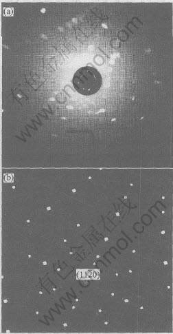
图2 垂直(Mo0.85Nb0.15)Si2单晶生长方向平面的
Laue衍射花样和C40( )面标准Laue花样
Fig.2 Laue diffraction pattern of (Mo0.85Nb0.15)Si2 crystal plane vertical to
its growth direction(a) and standard () plane of C40 structure (b)
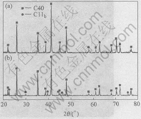
图3 (Mo0.85Nb0.15)Si2单晶和1600℃退火6h样品的X射线衍射谱
Fig.3 XRD patterns of (Mo0.85Nb0.15)Si2 single crystal (a) and sample
annealed at 1600℃ for 6h (b)
经1200~1700℃一系列退火处理后发现: 在1400℃以下, 合金保持C40结构不变(图4(a)); 当退火温度为1400℃时, 合金中出现C11b相(图4(b)); 延长退火时间, C11b相长大(图4(c)); 经1500℃退火6h后, 合金显微结构变为全片层状, 同时包含大晶粒的C11b相(图4(d)), 延长退火时间, C11b相不再继续生长, 但部分片层之间发生融合现象(图4(e)); 经1600℃退火6h后, 合金显微结构变为完全片层结构(图4(f)), 层间距为200~300nm(图4(h)); 经1700℃退火24h, 在合金中没有观察到C11b相的出现, 合金结构为C40(图4(g))。 表1列出了(Mo0.85Nb0.15)Si2 单晶与1600℃退火6h后合金中各相的成分。
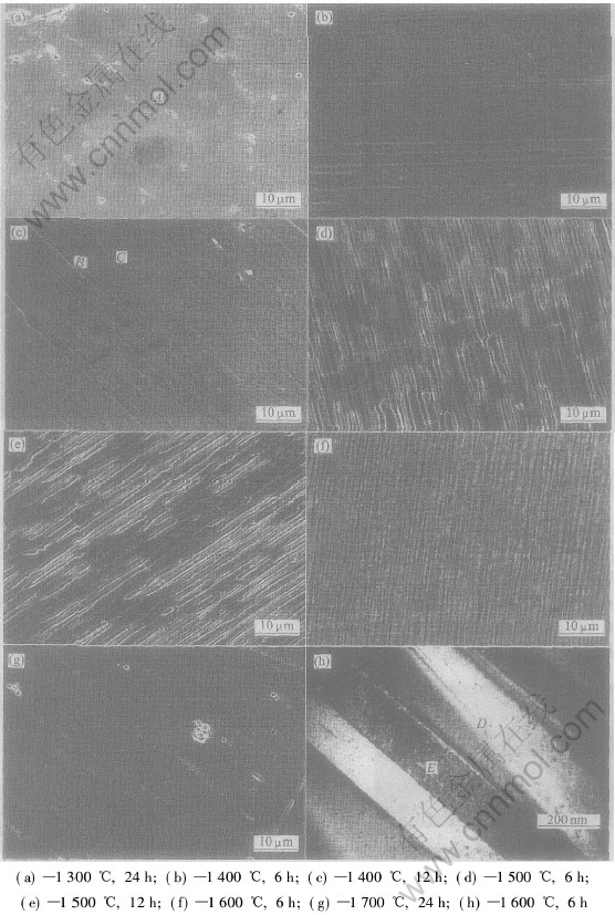
图4 (Mo0.85Nb0.15)Si2单晶经不同条件退火后的SEM形貌及TEM像
Fig.4 SEM morphologies (a-g) and TEM image(h) of (Mo1-xNbx)Si2 single crystal alloys annealed under different conditions
表1 (Mo0.85Nb0.15)Si2合金的EDS成分分析
Table 1 EDX analysis for spots indicated in Fig.4(a), 4(c), 4(h) of
(Mo0.85Nb0.15)Si2 alloy (mole fraction, %)

3 讨论
Umakoshi等[15]采用0.25mm/h的生长速率制备了(Mo0.85Nb0.15)Si2单晶, 采用5mm/h及10mm/h的生长速率均没有制得单晶, 而得到了MoSi2/NbSi2双相合金。 因此作者认为制备(Mo0.85Nb0.15)Si2单晶的极限生长速率应当在4~5mm/h之间。
1300℃以下对C40结构(Mo0.85Nb0.15)Si2单晶进行退火, 没有出现C40到C11b的相变, 这是因为在此温度范围内退火不能提供足够高的能量使原子进行迁移。 经1400℃退火, 出现了C40到C11b的相变, 这种相变可以认为是无核相变, 依靠合金中微小的成分起伏, 在Nb含量偏高处首先发生相变。 因此只在合金的某些区域形成了C11b相(图4(b))。 在此温度延长退火时间, 已形成的C11b相成为继续相变的核, 相变过程转变为有核相变, 观测到的结果就是在合金中出现了大块的C11b相与C40基体相交错分布的双相结构, 如图4(c)所示。 1600℃使得最初的C40到C11b的无核相变对成分的起伏更加敏感, 相变极易发生。 Umakoshi等[15]通过定向凝固制备了MoSi2/NbSi2双相合金, 在其制备的合金中, 除了C40和C11b相以外, 也包含了C40/C11b片层结构。 他们的研究表明, 片层结构中的C40相和C11b相存在着一定位向关系, 即 和[0001]C40 in lamellar∥[110]C11b in lamellar。 因此, 1500℃退火所导致的C40到C11b的相变必然使得新形成的C11b相与C40母相之间有严格的位向关系, 对合金的显微结构影响表现为形成取向一致的全片层结构(图4(d))。 在此温度范围延长退火时间, C11b相基本没有出现长大的现象, 而出现了在某些区域片层结构发生融合的现象。 这一现象的产生可能与片层结构的热稳定性有关, 对于片层结构热稳定性的研究目前还在研究当中。 与1500℃退火相比, 1600℃为相变提供了更高的能量, 可以看到1600℃退火6h后, 合金微观结构表现为非常密集的层片状结构, 层间距只有200~300nm(图4(f), 4(h))。 比较图4(c)和图4(h)中C40相与C11b相的成分可以发现, 经过相变后形成的C11b相都是贫Nb的, 但图4(h)中的C11b相所含的Nb含量更低, 这种更低Nb含量的C11b相的形成对于母相C40相的铌含量要求也低, 但是相变的发生却需要更高的能量。 可以想象, C11b相中的Nb含量低, 在合金总Nb含量不变的情况下, 必然能够形成更高的体积分数。 因此, 能够得到排列非常紧密的层状结构(图4(h))。 但是1700℃的退火却没有使得C40到C11b的相变发生。 作者认为1700℃已经超过了此相变发生的相转变温度。
到目前为止, MoSi2-NbSi2在高温区的伪二元相图还不清楚。 假设MoSi2-TaSi2与MoSi2-NbSi2有相似的相图, Nakano等[14]做出了MoSi2-NbSi2相图(如图5所示)。 对于(Mo0.85Nb0.15)Si2合金而言, 1700℃的温度已经到达了C40单相区, 因此在此温度即使退火24h亦不会发生相变, 合金依然保持C40结构不变(图4(g))。
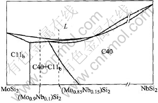
图5 根据MoSi2-TaSi2相图得到的MoSi2-NbSi2伪二元相图[14]
Fig.5 MoSi2-NbSi2 pseudo-binary phase diagram predicted from MoSi2-TaSi2 system[14]
4 结论
1) 1300℃以下退火, 对(Mo0.85Nb0.15)Si2单晶的组织结构没有影响。 C40到C11b的相变温度必须高于1300℃。
2) 1400℃退火形成了C40/C11b双相结构, C11b相随退火时间的延长长大。
3) 1500℃退火形成了C40/C11b全片层结构, 随退火时间延长部分片层结构出现融合现象。
4) 经1600℃退火6h后, 形成了紧密排列的C40/C11b全片层结构, 片层间距为200~300nm。
5) (Mo0.85Nb0.15)Si2合金在相图中C40与C40+C11b的转变温度约为1700℃。
REFERENCES
[1]Raj S V, Whittenberger J D, Zeumer B, et al. Elevated temperature deformation of Cr3Si alloyed with Mo [J]. Intermetallics, 1999, 7(7): 743-755.
[2]Sadananda K, Feng C R, Mitra R, et al. Creep and fatigue properties of high temperature silicides and their composites [J]. Mater Sci Eng A, 1999, A261(1-2): 223-238.
[3]Yamaguchi M, Inui H, Ito K. High-temperature structural intermetallics [J]. Acta Mater, 2000, 48(1): 307-322.
[4]Yoshimi K, Yoo M H, Wereszczak A A, et al. Yielding and flow behavior of Mo5Si3 single crystals [J]. Scripta Materialia, 2001, 45(11): 1321-1326.
[5]Mason D P, van Aken D C. On the creep of directionally solidified MoSi2-Mo5Si3 eutectics [J]. Acta Metall Mater, 1995, 43(3): 1201-1210.
[6]Maruyama T, Yanagihara K. High temperature oxidation and pesting of Mo(Si,Al)2 [J]. Mater Sci Eng A, 1997, A239-240(1-2): 828-841.
[7]Frankwicz P S, Perepezko J H. Phase stability of MoSi2 in the C11b and C40 structures at high temperatures[J]. Mater Sci Eng A, 1998, A246(1-2): 199-206.
[8]Shan A D, Wei F, Hitoshi H, et al. Microstructure and mechanical properties of MoSi2-X (X=Al, B, Nb) alloys fabricated by MA-PDS process [J]. Materials Transactions, 2002, 43(1): 5-10.
[9]Inui H, Ishikawa K, Yamaguchi M. Effects of alloying elements on plastic deformation of single crystals of MoSi2 [J]. Intermetallics, 2000, 8(9-11), 1131-1145.
[10]Petrovic J J, Vasudevan A K. Key developments in high temperature structural silicides [J]. Mater Sci Eng, 1999, A261(1-2): 1-5.
[11]Shaw L, Miracle K, Abbaschian R. Microstructure and mechanical properties of metal/oxide and metal/silicide interfaces [J]. Acta Metall Mater, 1995, 43(12): 4267-4279.
[12]Nakano T, Kishimoto M, Furut D, et al. Effect of substitutational elements on plastic deformation behaviour of NbSi2-based silicide single crystals with C40 structure[J]. Acta Mater, 2000, 48(13): 3465-3475.
[13]Boettinger W J, Perepezko J H, Frankwicz P S. Application of ternary phase diagrams to the development of MoSi2-based materials [J]. Mater Sci Eng A, 1992, A155(1-2): 33-34.
[14]Nakano T, Azuma M, Umakoshi Y. Microstructure and high-temperature strength in MoSi2/NbSi2 duplex silicides [J]. Intermetallics, 1998, 6(7-8): 715-722.
[15]Nakano T, Nakai Y, Maeda S, et al. Microstructure of duplex-phase NbSi2(C40)/MoSi2(C11b) crystals containing a single set of lamellae [J]. Acta Mater, 2002, 50(7): 1781-1795.
基金项目: 国家自然科学基金资助项目(50131030)
收稿日期: 2004-05-08; 修订日期: 2004-10-18
作者简介: 杨海波(1977-), 男, 博士研究生.
通讯作者: 杨海波; 电话: 021-62932440: 传真: 021-52540011; E-mail: yanghaibo@sjtu.edu.cn
(编辑陈爱华)

