Effect of growth-interrupted method on quality of AlGaAs/GaAs multiple quantum wells prepared by MBE
GUO Feng-yun(国凤云), WANG Huai-mang(王怀芒), ZHAO Lian-cheng(赵连城)
Department of Materials Physics and Chemistry, Harbin Institute of Technology, Harbin 150001, China
Received 10 April 2006; accepted 25 April 2006
Abstract: AlGaAs/GaAs multi-quantum well (MQW) was prepared by molecular beam epitaxy(MBE) with growth-interrupted heterointerface (GIH) method and continuous growth (CG) method, respectively. The microstructures of the MQWs were characterized by double-crystal X-ray rocking curve (DCRC) and atomic force microscopy (AFM), and the photoluminescence (PL) properties of the MQWs were also studied. The MQWs grown with GIH method show that higher order satellite peaks of Pendell?sung fringes are observed in DCRC, the roughness of surface is much reduced in AFM, and the full width at half maximum (FWHM) of exciton line is much narrower in PL. The results indicate that the GIH method reduces the monolayer growth step density at the heterointerface due to the migration of surface atoms for a few minutes growth interruption, and substantially improves the quality of AlGaAs/GaAs MQWs.
Key words: AlGaAs/GaAs multi-quantum wells; growth interruption; double-crystal X-ray rocking curve; atomic force microscope; photoluminescence
1 Introduction
Recently, AlGaAs/GaAs multi-quantum wells (MQWs) has been widely used for the fabrication of many kinds of high speed and high power semiconductor devices and photoelectronic devices, such as, AlGaAs/GaAs quantum well transistor with high electronic mobility, quantum well laser (QWL) and quantum well infrared photodetector (QWIP)[1, 2].
There are various aspects related to the quality of AlGaAs/GaAs quantum well to affect greatly the photoelectric properties of the corresponding devices, which include crystal defects, composition homogeneity, especially the roughness of interface and surface, and so on. To obtain a high performance QWIP or other devices, the quality of quantum well must be controlled carefully. Therefore, many studies have been done for the growth technology of AlGaAs/GaAs MQWs[3].
Molecular beam epitaxy(MBE) technique has been successfully used to prepare various kinds of multi-layer structures, including multi-quantum wells and superlattices, but some difficulties for high quality multi-layers growth have still existed[4].
In the present work, Al0.2Ga0.8As/GaAs MQW was grown on GaAs substrate by MBE with conventional continuous growth (CG) method and growth-interrupted heterointerface (GIH) method, respectively. The results show that the MQW grown with GIH method exhibits higher growth quality and better photoluminescence (PL) properties.
2 Experimental
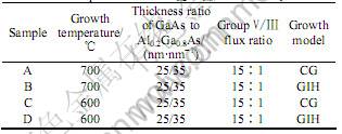
Al0.2Ga0.8As/GaAs MQWs were grown on a Riber Compact-21T MBE system, and the substrate was GaAs (001) with the off angle of 2?-4? toward [111] direction. The purities of MBE resource of Ga, As and Al rods were 99.999 99%. The buffer layer of GaAs with the thickness of 0.5 μm was grown on the substrate firstly, then the GaAs layer with the thickness of 25 nm and the Al0.2Ga0.8As layer with the thickness of 35 nm periodic structure with 11 periods were grown. The growth temperatures were 600 ℃ and 700 ℃,respectively. The cap layer was GaAs with the thickness of 25 nm. The detail growth parameters of the MQWs are listed in Table 1. The GIH was realized by shutting off the Ga source for 2 min at each heterointerface of the MQWs under the beam-equivalent pressure of As4 before proceeding with GaAs or AlGaAs deposition.
The double-crystal X-ray rocking curve (DCRC) measurements were performed on a Rigaku double-crystal X-ray rocking diffractometer with the reference crystal of bulk (400)Ge. The surface morphologies of the MQWs were investigated by using atomic force microscope(AFM) on a type Dimension 3100SPM AFM.
Table 1 Growth parameters of Al0.2Ga0.8As/GaAs MQWs

The PL measurements were carried out using a 32 cm grating monochrometor equipped with a cooled charge-coupled device camera. Ar ion laser was used as the PL excitation source with the wavelength of 514.5 nm, and the sample temperature was controlled at 10-300 K by using a He displex system.
3 Results and discussion
3.1 DCRC analysis
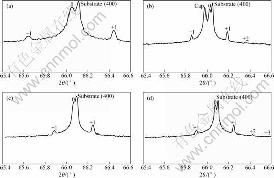
Fig.1 shows the results of the DCRC spectra of Al0.2Ga0.8As/GaAs MQWs, and the analysis results are listed in Table 2.
As it is well known, much important information related to the structure of multi-layers can be investigated through DCRC analysis. The sharper diffraction peak indicates the lower crystal defect density. Especially, the presence of clear Pendell?sung fringes is corresponding to more accurate periodic multi-layers and a high degree of perfection at the epitaxial layer interfaces and surface[5, 6].
Comparing the two samples, A and B, or C and D, grown at the same substrate temperature (700 ℃ or 600 ℃, respectively), it is clear that the quality of sample B (sample D) grown with GIH method is better than that of sample A (sample C) grown with CG method. The full width at half maximum (FWHM) of the former is narrower than that of the latter. In addition, the regular and well-resolved Pendell?sung fringes with higher intensities can be clearly observed on either side of the main satellite peaks in the MQWs grown with GIH method. So it can be concluded that AlGaAs/GaAs MQW grown with GIH method has smoother and more

Fig.1 DCRC spectra for samples A (a), B (b), C (c) and D (d)
Table 2 Analysis results of DCRC spectra of Al0.2Ga0.8As/GaAs MQWs

abrupt interface.
3.2 AFM analysis
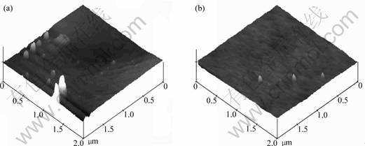
Fig.2 shows the results of the AFM surface morphologies of samples C and D, and the analysis results are listed in Table 3.
Table 3 Surface roughness of Al0.2Ga0.8As/GaAs MQWs

From the analysis of AFM, it can be found that the surface roughness of the MQWs grown with GIH method is much smaller than that of the MQWs grown with CG method. Indeed, the surface roughness of multi-layers is a presentation of interface roughness. It is clear that the low roughness surface is corresponding to the low roughness interface. When the film is grown with GIH method, the larger islands on the surface can grow through consuming the Ga and As atoms from small islands, because of the longer diffusing time on the surface of Ga and As atoms from the small islands to the larger ones in the case of GIH method. Therefore, the GIH method is an effective technology to reduce the interface roughness and surface roughness of MQWs growth.
3.3 PL analysis
The PL spectra of Al0.2Ga0.8As/GaAs MQWs measured at 10 K are shown in Fig.3, and the analysis results are listed in Table 4.

Fig.2 AFM images of samples C (a) and D (b)

Fig.3 PL spectra of Al0.2Ga0.8As/GaAs MQWs at 10 K: (a) Sample A; (b) Sample B; (c) Sample C; (d) Sample D
Table 4 Analysis results of PL spectra of Al0.2Ga0.8As/GaAs MQWs

The interface roughness at the atomic level plays an important role in the optical properties of AlGaAs/GaAs MQWs[7, 8]. The low-temperature PL measurements reveal that a rough interface manifests itself in inhomogeneous broadening of the exciton linewidth in the PL spectra especially for a quantum well with reduced well width[9]. The narrower and sharper PL spectral peaks with higher intensity suggest that the MQW has smoother and more abrupt interface as well as lower density of crystal defects[10, 11].
In Fig.3, the dominant PL of the samples (A, B, C and D) originates from the recombination of the first heavy hole with the first electronic subband (E1-HH1) in the GaAs well[12]. The results show that the PL intensity of sample B (sample D) is about 10 times greater than that of sample A (sample C) and the FWHM of the former is narrower than that of the latter, indicating that sample B(sample D) grown with GIH method has smoother and more abrupt heterointerfaces. This agrees with the DCRC and AFM measurements obtained above.
4 Conclusions
The structural quality of Al0.2Ga0.8As/GaAs MQWs grown with GIH method can be improved substantially in comparison with CG method, including the interface roughness, surface roughness, and density of crystal defects. In addition, the PL properties of the MQWs grown with GIH method are also enhanced greatly. GIH method is an effective method to obtain AlGaAs/GaAs MQWs with high quality. The interruption technique during MBE growth under As pressure is applicable to the fabrication of devices with an extremely smooth and abrupt heterointerface.
Acknowledgements
The authors gratefully acknowledge helpful discussions with professor FEI Wei-dong of Harbin Institute of Technology.
References
[1] SAKAMOTO M, ENDRIZ J G, SCIFRES D R. 120W CW output power from monmlithic AlGaAs (800 nm) laser diode array mounted on diamound heatsink[J]. Electronics Letters, 1992, 28: 197-199.
[2] ROGALSKI A . Infrared detectors: status and trends[J]. Progress in Quantum Electronics, 2003, 27: 59-210.
[3] CHAND N. Growth of high quality AlGaAs/GaAs heterostructures by molecular beam epitaxy for photonic and electronic device applications[J]. Thin Solid Films, 1993, 231: 143-157.
[4] FOXON C T. Three decades of molecular beam epitaxy[J]. Journal of Crystal Growth, 2003, 251: 1-8.
[5] HOLLANDERS M A, THIJSSE B J. Layer thickness variations and X-ray disffraction patterns: a geneal treatment[J]. J Appl Phys, 1991, 70(6): 1270-1275.
[6] TOMICH D H, MITCHEL W C, CHOW P, TU C W. Study of interfaces in GaInSb/InAs quantum wells by high-resolution X-ray diffraction and reciprocal space mapping[J]. Journal of Crystal Growth, 1999, 201: 868-871.
[7] BIMBERG D, CHRITEN J, FUKUNAGA T, NAkAS H, et al. Cathodoluminescence atomic scale images of monolayer islands at GaAs/GaAlAs interfaces[J]. J Vac Sci Technol, 1987, 4: 1191-1193.
[8] HARRIS C I, MONEMAR B, KALT H, HOLTZ P O. Influence of interface localization on the binding energy of acceptor bound excitons in narrow GaAs/AlxGa1-xAs quantum wells[J] . Phys Rev B, 1995, 51(19): 13221-13225.
[9] NAKASHIMA H, TAKEUCHI T, INOUE K, et al. Photo- luminescence and photoluminescence excitation of AlGaAs/GaAs quantum wells with growth-interrupted heterointerface grown by molecular beam epitaxy[J]. Superlattices and Microstructures, 1997, 22 (4): 511-515.
[10] TANAKA M, SAKAKI H. Atomistic models of interfaces structures of GaAs-AlxGa1-xAs (x=0.2-1) quantum wells grown by interrupted and uninterrupted MBE[J]. Journal of Crystal Growth, 1987,81: 153-158.
[11] KLANN R, GRAHN H T, FUJIWARA K. Exciton dynamics within growth islands of GaAs/Al0.17Ga0.83As single quantum wells[J]. Phys Rev B, 1995, 51(15): 10232-10235.
[12] OH Y T, KANG T W, KIM T W. Comparison of the interdiffusion lengths in GaAs/Al0.35Ga0.65As multiple quantum wells determined from photoluminescence and double crystal X-ray rocking curve measurements[J]. Applied Surface Science, 1998, 135: 238-242.
(Edited by CHEN Wei-ping)
Corresponding author: GUO Feng-yun; Tel: +86-451-86418622; Fax: +86-451-86413922; E-mail: guowen@hit.edu.cn