
Si3N4 nano-microsphere synthesized by cathode arc plasma and heat treatment
GENG Zhong-rong(������)1, YAN Peng-xun(����ѫ)2 , FAN Duo-wang (������)1, YUE Guang-hui (�����)2
1. National Engineering Research Center for Technology and Equipment of Green Coating,
Lanzhou Jiaotong University, Lanzhou 730070, China;
2. Institute for Plasma and Metal Materials, Lanzhou University, Lanzhou 730000, China
Received 10 August 2009; accepted 15 September 2009
Abstract: The Si3N4 microcrystals with a hollow sphere structure were prepared by using the simple heat treatment of the Si3N4 flakes, which were prepared by using the cathode arc plasma. The products were characterized by XRD, SEM and TEM. The photoluminescence (PL) spectrum of the Si3N4 nano-microsphere was studied. The obtained Si3N4 microcrystals, which show a hollow sphere structure, are up to several nanometers in diameter. During the process, the heat treatment and Ni catalyst play a key role in the forming structure and morphology. This result provides a possibility for mass producing Si3N4 microcrystals.
Key words: Si3N4 hollow sphere; heat treatment; photoluminescence; cathode arc plasma
1 Introduction
Silicon nitride (Si3N4) is an advanced ceramic material, and it has many potential applications due to its good performance in mechanical, chemical, electronic, and thermal applications[1]. Being an important member of the promising semiconductors of nitrides (such as GaN and AlN), Si3N4 is also a wide band gap (about 5.3 eV) semiconductor. In addition, the dopant-treating Si3N4 compounds are widely used in the microelectronics industry for various applications as the optical devices[2].
As a result, the synthesis of difform Si3N4 nanomaterlais has received extensive attention in recent years and various synthesis routes have been proposed. Recently, the three kinds of known polymorphs of ��-Si3N4, ��-Si3N4 and c-Si3N4 with a spinel structure have been prepared[3-7]. By using ammonia microwave plasma heating, the Si3N4 nanoneedles grown on silicon were prepared[8]. And the Si3N4 nanorods were synthesized with the mild benzene-thermal route as the template[9]. Si3N4 nanowires and Si3N4 single-crystalline nanobelts were achieved by a vapor-solid thermal reaction with nammonia and silicon monoxide[10]. the large-scale synthesis of single-crystalline Si3N4 nanobelts with high yield via catalyst-assisted pyrolysis of polymeric precursor. The growth mechanism of the nanobelts was also proposed[11]. The Si3N4 whiskers with dendritic and riblike structure were achieved by a chemical vapor deposition technique[12-13]. Branched Si3N4 whiskers have been fabricated via catalyst-assisted pyrolysis of polymeric precursors[14]. To date, one-dimensional Si3N4 nanostructures have been synthesized via different methods. However, the simple and massive production of Si3N4 microcrystals are still not proposed.
In this work, the Si3N4 microcrystals with a hollow sphere structure were prepared. A simple and novel route for the preparation of Si3N4 nano-microsphere with urchin-like structure by heat treatment was reported. The optical properties of as prepared Si3N4 nano-microsphere were discussed.
2 Experimental
Before the preparation of Si3N4 nano-microsphere, Si3N4 flakes were synthesized by cathode arc plasma, which is one of the most powerful methods because of uniform particles and high efficiency, using Si powder and nickel nanopowder with a molar ratio (100?1) in pure nitrogen atmosphere. The nickel nanopowder acted as the catalyzer in the reaction. The mixture of pure silicon powder and nickel nanopowder served as the anode, and
a tungsten rod served as the cathode. After the vacuum level of the chamber was up to 10 Pa, the pure nitrogen gas was introduced into the chamber as the reaction gas. During the preparing process, the pressure of the chamber was 2.0��103 Pa, the arc discharge voltage was 40 V and the current was 40 A. The arc discharge was maintained for 10 min to evaporate the mixture. The black Si3N4 flakes powders were obtained. Then, the black Si3N4 flakes were calcined in a quartz tube furnace at 500 �� for 5 h in argon atmosphere and the offwhite Si3N4 nano-microsphere powders were obtained.
The structure of the sample was measured by X-ray diffraction (XRD) on a Rigaku D/Max-2400 diffractometer with monochromatized Cu Ka radiation (l=0.154 056 nm) and ��-2�� scan. Transmission electron microscopy (TEM) examination was carried out by using a Hitachi H-600 transmission electron microscope operated at 100 kV with a nominal point-to-point resolution of 0.23 nm. The morphology observation was performed on field emission scanning electron microscope (FE-SEM, Hitachi S-4800). Photo- luminescence (PL) measurements were carried out at the room temperature by using the pulsed (5 ns) RF-5301 laser with the excitated wavelength of 280 nm. The experiment with similar conditions was also carried out without the Ni powder additive for comparison.
3 Results and discussion
Fig.1 shows the XRD pattern of the Si3N4 nano-microsphere. The diffraction peaks can be indexed to the orthorhombic structure of Si3N4, which exactly accords with the reported values of JCPDS card No. 76-1408. The impurity peaks suggest that the Si powder reacts incompletely with nitrogen.
The structural analysis of the nano-microsphere was performed by using TEM and SEM. Fig.2(a) shows the SEM image of the Si3N4 nano-microsphere obtained by
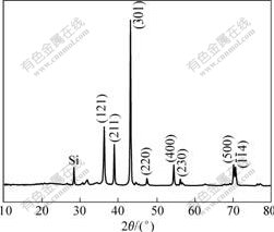
Fig.1 X-ray powder diffraction pattern of Si3N4 hollow
heat treatment of Si3N4 flakes for 5 h. Fig.2(b) shows the TEM image of the Si3N4 nano-microsphere with diameters around 2 ?m��and the image also confirms that the Si3N4 nano-microsphere is in hollow structure.
Fig.3(a) shows the TEM image of as-prepared Si3N4 flakes and the corresponding SAED pattern (inset of Fig.3(a)). It can be seen that Si3N4 flakes take on a flake-like morphology, and the SAED pattern of the flake shows that it consists of several layers. It is believed that the special structure of the Si3N4 flakes plays an important role in the following transformation.
The heat treatment plays an important role in the structure and morphology of Si3N4 nano-microsphere. Fig.3 shows the evolution of morphology during the heat treatment. Fig.3(b) shows that the flakes begin to bend and kink when they are calcined at 500 �� for 1 h. Fig.3(c) shows the TEM image of the product after being calcined for 3 h. It can be seen that the structure is broken down into amorphous aggregations and the amorphous turns into erose nano-microsphere. As shown in Fig.3(d), when the calcination time increases to 5 h, most of the amorphous turn into the nano-microsphere and come to separate from the amorphous.
It is noticed that if the electron beam intensity of TEM is strong enough, the spheres would splittingly fall
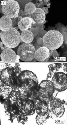
Fig.2 SEM image (a) and TEM image (b) of product calcined for 5 h
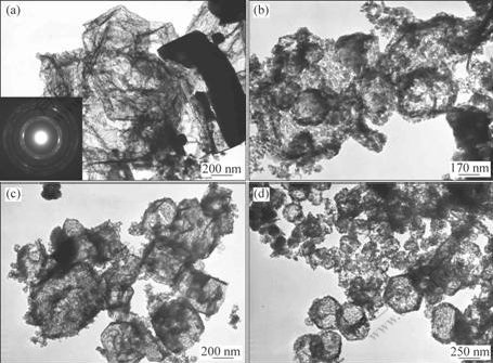
Fig.3 Morphologies of product obtained under heat treatment for different times: (a) As-prepared Si3N4 flakes; (b) Product calcined for 1 h; (c) Product calcined for 3 h; (d) Product calcined for 5 h
apart into small nanosheets. When the electron beam intensity of TEM is lower than critical stable value, those small nanosheets would form into new spheres.
From the above experimental results, the formation mechanism of Si3N4 hollow spheres is suggested as shown in Fig.4. When the precursors with structure of flakes are obtained by the arc discharge treatment, one side of the flake��s surface shows electronegative quality and the other side shows electropositive quality for their structure reason. So several flakes are superposed
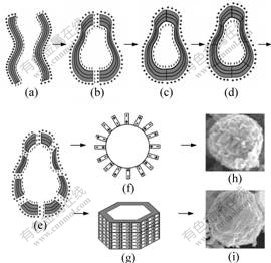
Fig.4 Schematic illustration of hierarchical structure of formation mechanism of Si3N4 hollow spheres
(Fig.4(a)). During the annealing, two flakes are connected to form an erose hollow sphere (Figs.4(b) and 4(c)). With the increase of the annealing temperature, the erose hollow spheres break up and recrystallize (Fig.4(d) and 4(f)). As to the minimum surface energy and surface tension of the sphere and hexahedron, the broken flakes are reassembled and turn into sphere and hexahedron (Figs.4(g) and (i)). However, the exact mechanism is still unknown and needs further investigation.
We also studied the PL properties of the Si3N4 nano-microsphere obtained in the experiment. Fig.5 shows the PL spectra of the Si3N4 nano-microsphere using the excitation line at 280 nm measured at room temperature. The spectra ranging from 300 nm to 600 nm
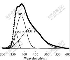
Fig.5 Room-temperature PL spectra of Si3N4 hollow spheres
are smoothened and deconvoluted into several Gaussian peaks, as shown in Fig.5. From the PL spectrum of the Si3N4 nano-microsphere, a strong violet emission peak centered at 385.5 nm (3.19 eV) is observed, and other strong emission peaks are also observed at 363.7 nm (3.38 eV) and 431.8 nm (2.85 eV).
It is obvious that these intensive light emissions from Si3N4 nano-microsphere are not the direct band gap emission, but are generally attributed to the deep-level or trap-level defects. According to Robertson and Powell��s report[15], there are four principal defects closely related to its light emission, including the Si and N dangling bonds (��Si�D and ��N�D), ��Si�DSi��, ��N0, ��Si0. There are two nitrogen defective conditions that give rise to the levels within the gap, namely N4+ and N20, which were calculated to close to the conduction and valence band respectively. The presence of the nitrogen dangling bond defect was confirmed by spin resonance measurements. According to Deshpande��s report[16], the recombination process at the silicon dangling bond is due to the rise of the broad (2.5��0.1) eV peak, and the (3.0��0.1) eV peak is due to recombination either from the conduction band to the N20 level or the valence band to the N4+ level. So the luminescence at 431.8 nm (2.85 eV) is possibly caused by recombination process at the silicon dangling bond. The luminescence at 385.5 nm (3.19 eV) and 363.7 nm (3.38 eV) are possibly caused by the electronic recombination either from the conduction band to the N20 level or the valence band to the N4+ level.
4 Conclusions
1) A very simple and scalable pathway towards Si3N4 nano-microsphere is achieved. The Si3N4 nano-microsphere is prepared via heat treatment of the Si3N4 flakes at 500 �� for 5 h in argon atmosphere.
2) The Si3N4 flakes are prepared by using the cathode arc plasma. It is found that the heat treatment and Ni catalyst play an important role in the forming of structure and morphology.
3) An intensive broad blue light emission peak at 385.5 nm and other strong broad light emission peak at 363.7 nm and 431.8 nm are observed from the room-temperature PL spectrum. The current results can lead to a new and simple way for mass production of Si3N4 microcrystals.
References
[1] DANNIEL M, MARTIN D P, ROBIN A L D, HELEN P, DON S. Microstructure of an extruded ��-silicon nitride whisker reinforced silicon nitride composite [J]. J Am Ceram Soc, 1992, 75(10): 2713-2718.
[2] XU Y J, CAO C B. Preparation of novel saw-toothed and riblike ��-Si3N4 whiskers [J]. The Journal of Physical Chemistry B, 2006, 110(7): 3088-3092.
[3] ZERR A, MIEHE G, SERGHIOU G, RIEDEL R, FUESS H, KROLL P, BOEHLER R. Synthesis of cubic silicon nitride [J]. Nature, 1999, 400(22): 340-342.
[4] TAKEHIKO H, KATSUNORI A, TATSUO M. Synthesis of ��-Si3N4 particles from ��-Si3N4 particles [J]. Journal of the European Ceramic Society, 2000, 20(8): 1191-1195.
[5] YANG Yun, CHEN Yi-xiang, ZHI Ming-lin, LI Jiang-tao. Synthesis of ��-Si3N4 using low-a-phase Si3N4 diluent by the seeding technique [J]. Scripta Materialia, 2007, 56(5): 401-404.
[6] BELMONTE M, MIRANZO P, ISABEL O M. A method for disentangling ��-Si3N4 seeds obtained by SHS [J]. Powder Technology, 2008, 182(3): 364-367.
[7] GOULD D A, QUINLAN M, ALBANO M P, GARRIDO L B, GENOVA L A, PLUCKNETT K P. A simple method for synthesis of acicular ��-Si3N4 seed crystals [J]. Ceramics International, 2009, 35(4): 1357-1362.
[8] CUI H, STONER B R. Nucleation and growth of silicon nitride nanoneedles using microwave plasma heating [J]. J Mater Res, 2001, 16: 3111-3115.
[9] XU F, ZHANG X, XI W, HONG J, XIE Y. Growth of pure ��-Si3N4 nanorods from the synergic nitrogen sources [J]. Chemistry Letters, 2003, 32(7): 600-602.
[10] XU Ya-jie, CAO Chuan-bao, DU Hong-li, LI Jie, ZHU He-sun. Synthesis and photoluminescence of belt-shaped Si3N4 whiskers [J]. Materials Letters, 2007, 61(18): 3855-3858.
[11] WANG Feng, JIN Guo-qiang, GUO Xiang-yun. Sol-gel synthesis of Si3N4 nanowires and nanotubes [J]. Materials Letters, 2006, 60(3): 330-333.
[12] CHEN L P, GUO D T J, SHAW D T. High-density silicon and silicon nitride cones [J]. Journal of Crystal Growth, 2000, 210(4): 527-531.
[13] BAI Yu-jun, WANG Cheng-guo, QI Yong-xin, ZHU Bo, WANG Yan-xiang, LIU Yu-xian, GENG Gui-li. Rapid synthesis of Si3N4 dendritic crystals [J]. Scripta Materialia, 2006, 54(3): 447-451.
[14] YANG W Y, XIE Z P, LI J J, MIAO H Z, ZHANG L G, AN L N. Growth of platelike and branched single-crystalline Si3N4 whiskers [J]. Solid State Communications, 2004, 132(3/4): 263-268.
[15] ROBERTSON J, POWELL M J. Gap states in silicon nitride [J]. Applied Physics Letters, 1984, 44(4): 415-417.
[16] DESHPAND E, SADANDAND V, GULARI E, BROWN S W, RAND S C. Optical properties of silicon nitride films deposited by hot filament chemical vapor deposition [J]. Journal of Applied Physics, 1995, 77(12): 6534-6541.
(Edited by YANG You-ping)
Foundation item: Project(60376039) supported by the National Natural Science Foundation of China
Corresponding author: GENG Zhong-rong; Tel: +86-931-4956036; E-mail: gzrong-1977@163.com