
In-situ monitoring of nickel electrodeposit structure using
electrochemical noise technique
YANG Zhong-nian(杨仲年)1, ZHANG Zhao(张 昭) 1, LENG Wen-hua(冷文华) 1,
LING Ke(凌 克) 1, ZHANG Jian-qing(张鉴清)1,2
1. Department of Chemistry, Zhejiang University, Hangzhou 310027, China;
2. State Key Laboratory for Corrosion and Protection, Shenyang 110015, China
Received 19 May 2005; accepted 28 August 2005
Abstract: The nickel electroplating process was investigated by means of electrochemical noise(EN), cyclic voltammetry in conjunction with the scanning electron microscopy(SEM) technique. The results show that, in the experimental conditions and with the increase of current density, the growth mechanism of nickel crystallites changes from 2-D to 3-D with the potential turning point of about -1.15 V, and the potential for the onset of diffusion control of the ensemble nickel electroplating process was about -1.4 V. In the case of activation-control, the two-dimensional (2-D) nucleation / growth process of nickel often results in the electrocrystallization EN features of only slowly small positive potential drift and the corresponding compact layer-by-layer deposit structure, and the maximum relative energy of the RP-EDP (re-plotted relative energy distribution plot), which is obtained from wavelet analysis, defined in the region with smaller scales. While under the diffusion-control, the three-dimensional (3-D) nucleation / growth process of nickel, often results in the electrocrystallization EN features of both the fast positive potential drift and subsequent remarkable negative potential drift and the corresponding dentritic/large conglomerate structure of nickel deposit, and the maximum relative energy of the RP-EDP defined in the region with larger scales. The electroplating time affects the nickel deposit structure mainly through its influence on the growth rate of crystallites and the Ni2+ ions diffusion process around each crystallite.
Key words: nickel electroplating; electrochemical noise; electrodeposit structure
1 Introduction
Electrocrystallization EN is not an unknown phenomenon and has been reported in literatures for several electroplating systems[1-6]. For examples, in the case of zinc electroplating which can lead to spongy, compact or dentritic deposits, the experimental study of the electrocrystallization current EN allows us to establish some close correlations between the deposit morphology and the noise power measured in the low frequency range[7]. In the case of nickel deposition, the noise power  for time zero is proportional to
  (I is the electroplating current density), where the exponent α is approximately 2 for the [110] orientation, whereas it is lower than 1 for the [211] orientation[7].
EN analysis can be performed in time domain[8], frequency domain[9, 10], or using statistical method[11] and wavelet technique[12-16], etc. Recently, our research group explored the relationship between the features of RP-EDP, which is obtained from the powerful wavelet transform technique, and the zinc deposit structure, and found that the RP-EDP can be used as ‘fingerprints’of EN to characterize the electro-plating process and the deposit structure[17].
The aim of this work is to monitor the nickel electrodeposits structure using EN technique, especially investigate the relationship of the crystallite growth type (2-D/3-D growth type) with the electrocrystallization EN features obtained from wavelet analysis and the corresponding nickel electrodeposits structure phenomenologically.
2 Experimental
The galvanization bath electrolyte was prepared with AR grade reagents and de-ionized water according to the composition shown in Table 1. A conventional glass electrolysis cell with provision for inlet and outlet for deaerating the solution with N2 gas was used. A three-electrode system consisting of 1) disc brass copper electrode (59.65Cu40.35Zn, mass fraction, %) with an area of 0.502 7 cm2 exposed used as working electrode(WE), 2) saturated calomel (reference) electrode(SCE) and 3) a large bright platinum foil as the counter electrode, was employed. Before measurements, the exposed surfaces of the WE were polished using silicon carbide papers from 3 through 1 to 0.5 μm and velvet, rinsed with the de-ionized water, washed in acetone, rinsed with the de-ionized water again and then dried in air. Each experiment was repeated at least three times to verify the reproducibility of the results.
Table 1 Composition of galvanization bath electrolyte and deposition conditions
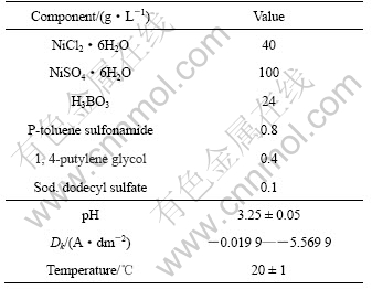
During zinc electroplating performed under galvanostatic control by EG & G PARC 173 potentiostat/galvanostat, the electrocrystallization noise data were recorded with a commercial PowerLab coupled with GP Amp (ADInstruments Pty Ltd, Australia) at a sampling rate of 10 Hz. Cyclic voltammetry was performed with a commercial Model 660A electrochemical analyzer/workstation (CH Instruments Inc., US). Just after the EN experiments, scanning electron microscopy (SEM, HITACHI S-570, Japan) was used to observe the morphologies of the electrodeposits. The experimental temperature was controlled by thermostat water tank at (20±1)℃ and the experimental device was shielded in a Faradic cage. All potentials (in this paper) were referred to SCE.
3 Results and discussion
3.1 Relation of 2-D/3-D growth with EN features and corresponding deposit structure
The nickel electroplating process was first investigated using cyclic voltammetry at a scan rate of 5 mV/s. The sweep potential range was from open circuit potential to different scan reversal potential(Figs.1 and 2) and always initiated in the negative direction. From Fig.1 it can be seen that, with the negative increase of the scan reversal potential, the nucleation/growth mechanism of nickel changed from two-dimensional (2-D) to three-dimensional (3-D) [18, 19] and the turning point was about -1.15 V.
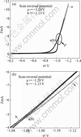
Fig.1 Discrimination between 2-D and 3-D growth of nickel electroplating: (a) Cyclic voltammogram; (b) Enlargement of point P in Fig.1(a)
Meanwhile, when changing the scan reversal potential anodically, the cross-potential shifted cathodically(Fig.2). According to the studies of Fletcher[18], the phenomenon of the negative drift of the cross-potential with the positive increase of the scan reversal potential indicates the onset of diffusion control. Consequently, in our case and when cathodic potential increased negatively to about -1.4 V, the ensemble nickel electroplating process should be controlled by diffusion of Ni2+ ions from the bulk solution to the nucleation/growth points. From Fig.2(c), it can be seen that another interesting phenomenon occurred, i.e. when the scan reversal potential was more negative than the peak potential in the voltammogram (Fig.2(a)), the cross-potential kept at a relative steady value (Fig.2(c)). The reason is under further investigation.
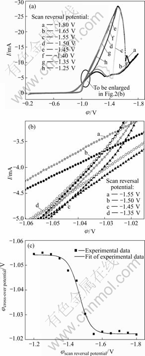
Fig.2 Determination of onset of diffusion control of nickel electroplating process
Fig.3 shows the typical cyclic voltammogram of brass substrate in the blank electrolyte without Ni2+. When comparing Fig.1 with Fig.3, it can be concluded that the current from -0.80 V to the peak potential in the voltammogram should be mainly attributed to the nickel electrodeposition. Meanwhile, from Figs.1 and 2, no anodic dissolution peaks can be observed and little information about the nickel electrodeposits structure can be obtained. Consequently, the nickel electroplating process was furthermore investigated using electrochemical noise technique.
Figs.4-8 show the EN features in time domain and the corresponding characteristics of the nickel deposit structure. It can be seen that the deposit structure changes from large conglomerate/dentritic particles to compact layers with the decrease of current density from about -5.57 A/dm2, which is the value corresponding to the cathodic current peak in Fig.2 to about -0.02 A/dm2.
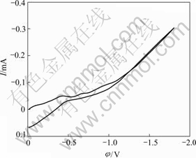
Fig.3 Cyclic voltammogram of copper electrode in blank electrolyte without Ni2+ ions
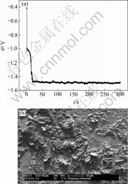
Fig.4 EN generated during nickel electroplating(a) and corresponding SEM image of deposit(b) at Dk=-5.569 9 A/dm2, t=5 min
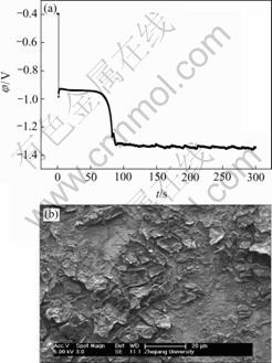
Fig.5 EN generated during nickel electroplating(a) and corresponding SEM image of deposit(b) at Dk=-5.172 1 A/dm2, t=5 min
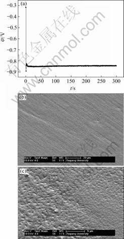
Fig.6 EN generated during nickel electroplating(a) and corresponding SEM images of deposit(b) at Dk=-2.387 1 A/dm2, t=5 min
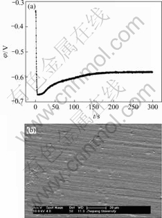
Fig.7 EN generated during nickel electroplating(a) and corresponding SEM image of deposit(b) at Dk=-0.079 6 A/dm2, t=5 min
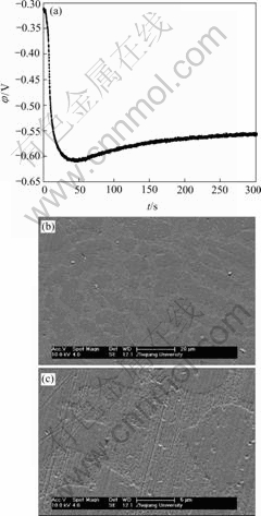
Fig.8 EN generated during nickel electroplating(a) and corresponding SEM images of deposit(b, c) at Dk=-0.019 9 A/dm2, t=5 min
In order to probe into the relationship between the features of electrocrystallization EN generated during the nickel electroplating and the electrodeposits structure in more details, and develop an in-situ method to examine the electrodeposits quality, the time-domain EN data in Figs.4-8 were analyzed using FWT (Fast wavelet technique) and based on the study of ABALLE[12-14] and our previous work[16, 17]. Before performing FWT analysis, the time-domain data were pretreated according to the method depicted in our previous work[17] to effectively eliminate the influence of the current contribution caused by capacitance charging, and the ensemble energy of the noise is calculated as follows:
 (n=1, 2, …, N) (1)
Then, the fraction of energy associated with each crystal can be calculated by
 (l=1, 2, …, J, J=8) (2)
 (l=1, 2, …, J) (3)
Since the chosen wavelets are orthogonal, the following equation is satisfied[12-17].
 (4)
(4)
In Eqns.(1)-(4), all symbols have the same meaning as depicted in Ref.[17]. Meanwhile, in order to remove the energy contribution of DC drift from the ensemble energy of the noise and probe the energy contribution from the D series crystals, which mainly reflect the information of the fast nucleation/growth process during nickel electroplating, the EDP (the plots of the relative energy accumulated by each crystal vs the crystal name) obtained from Eqns.(1)-(4) was re-plotted by discounting the contribution of S8 crystal from the ensemble signal energy, i.e. removing the large voltage transient from the raw data. Fig.9 illustrates the corresponding RP-EDP (re-plotted EDP) of the noise data shown in Figs.4-8.
Generally, the RP-EDP can be divided into the following three segments: 1) region A between D1 and D3 mainly characterizes the nucleation process, 2) region B between D3 and D6 mainly characterizes the growth process, and 3) region C between D6 and D8 mainly reflects the information about the diffusion process[17]. Consequently, it can be concluded that, with the decrease of current density, the maximum relative energy defined from D8 to D1 crystal (Fig.9) indicates that the rate determining step of the ensemble electroplating process changed from diffusion-control through mixed-control to activation-control, which resulted in that the corresponding deposit changed from the dentritic/large conglomerate structure to compact layer (Figs.4-8).
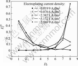
Fig.9 RP-EDP corresponding to potential noise of Figs.4-8
Therefore, when the current density (Dk) was sufficiently low (such as -0.019 9 A/dm2), the ensemble electroplating process was only controlled by electrochemical polarization (Fig.9) and the nickel deposition followed the 2-D layer-by-layer growth mechanism (Fig.1) that can be obviously observed in Fig.8(c). In this case, the imperfections such as plateau edges, kinks, vacancies and emergent screw dislocations[20], which existed on the newly formed deposit layer, would trigger the nucleation/growth of new crystallites at these sites and resulted in the surface morphology as shown in Fig.8(b). When the current density increased to -0.079 6 A/dm2, the relative energy accumulated in region C increased in spite of the fact that the maximum relative energy still defined in region A (Fig.9). The reason may be that the high current density would result in much more and much larger imperfections on the deposit surface (Fig.7(b)), at which the growth of many newly formed crystallites would lead to the local diffusion of Ni2+ ions and resulted in the onset of 3-D growth (Fig.1). For the case of Dk=-2.387 1 A/dm2, the nickel deposition was controlled by both activation and diffusion (Fig.9) and followed the 3-D nucleation and subsequent grain growth mechanism (Fig.1). In these conditions, the nucleation/growth rate of crystallites increased fast, which resulted in the increase of crystallites and the local diffusion around each crystallite, however many growing crystals amalgamated together as can be seen from Fig.6(c) and resulted in the compact deposit layer (Fig.6(b)). When the current density increased to the value (such as Dk=-5.172 1 A/dm2) where the nickel electroplating was mainly controlled by diffusion, the concentration of electrochemically active positive ions (Ni2+) adjacent to the cathode, especially in the double layer decreased sharply, and the electrochemically active positive ions reached the cathode surface would discharge preferentially on the homogeneous crystallites or the inhomogeneous sites like emergence points of edge, screw dislocation and kink sites, etc, where the surface Gibbs free energy is relatively high, which resulted in the dentritic/conglomerate structure of nickel deposit (Fig.4(b) and Fig.5(b)).
Based on the results of Figs.1 and 2 and Figs.4-9, it can also be rationally deduced that the 2-D nucleation/growth process of nickel, which is under the activation-control, often results in the compact deposit layer and possesses the electrocrystallization EN feature of only small positive potential drift due to the nucleation/growth of crystallites. While the 3-D nucleation/growth process of nickel, which is under diffusion-control, often results in the dentritic/large conglomerate structure of nickel deposit and possesses the electrocrystallization EN features of both the positive potential drift and subsequent remarkable negative potential drift, while the latter may be attributed to the synergism of both diffusion and the fact that the electrode potential of nickel is much less than that of copper.
3.2 Evolution features of EN and corresponding deposit structure with time
Figs.10-13 show the evolution features of electro- crystallization EN in time-domain and corresponding deposit structure, while Fig.14 shows the corresponding RP-EDP features of the noise shown in Figs.10-13. It can be clearly seen that, the electroplating time affected the nickel deposit structure (Figs.10-13) mainly through its influence on the growth rate of crystallites and the diffusion process around each crystallite (Fig.14).
Because that Dk=-4.774 2 A/dm2, nickel electro- plating was mainly controlled by diffusion of electrochemically active positive Ni2+ ions (Figs.1, 2 and 14). When the cathodic current was applied on the electrode and in the case of shorter electroplating time,
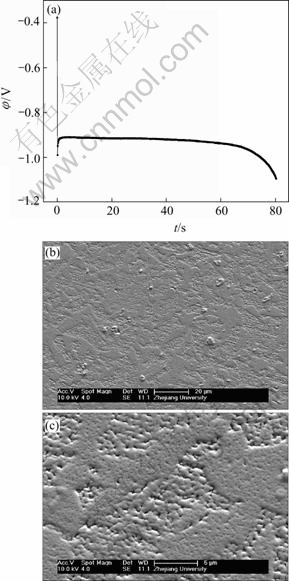
Fig.10 EN generated during nickel electroplating(a) and corresponding SEM images of deposit(b, c) at Dk=-4.774 2 A/dm2, t=80 s
many crystallites nucleated simultaneously. However, as mentioned above, the electrochemically active positive ions (Ni2+) reached the cathode surface would discharge preferentially on the homogeneous previously formed crystallites or the inhomogeneous sites like emergence points of edge, screw dislocation and kink sites, etc, where the surface Gibbs free energy was relatively high, which caused the serious local diffusion of Ni2+ ions around the newly formed crystallites and resulted in the maximum relative energy defined in region C (Fig.14). With the increase of electroplating time, the local diffusion region of Ni2+ ions around each newly formed crystallites would merge together and finally evolved into a thick diffusion layer above the whole cathode,
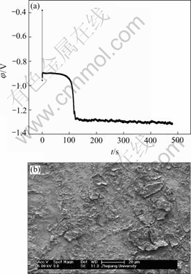
Fig.11 EN generated during nickel electroplating(a) and corresponding SEM image of deposit(b) at Dk=-4.774 2 A/dm2, t=8 min
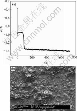
Fig.12 EN generated during nickel electroplating(a) and corresponding SEM image of deposit(b) at Dk=-4.774 2 A/dm2, t=12 min
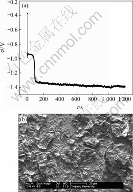
Fig.13 EN generated during nickel electroplating(a) and corresponding SEM image of deposit(b) at Dk=-4.77 42 A/dm2, t=20 min
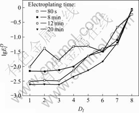
Fig.14 RP-EDP corresponding to potential noise of Figs.10-13
which resulted in the decrease and increase of the relative energy accumulated in region A and region C respectively.
4 Conclusions
The influence of electroplating current density and electroplating time on the features of electrocrystallization EN and the corresponding nickel deposit structure was investigated based on the wavelet technique. With the increase of current density, the growth mechanism of nickel crystallites should change from 2-D to 3-D, the potential turning point was about -1.15 V. Under activation-control, the 2-D growth type of nickel deposit possessed the EN features of the slowly positive potential drift, the corresponding nickel deposit layer was compact and the maximum relative energy accumulated in the region of RP-EDP with smaller scales. While under diffusion-control, the 3-D growth type of nickel deposit possessed the EN features of the fast positive potential drift and subsequent remarkable negative potential drift, the corresponding nickel deposit layer was dentitric and the maximum relative energy accumulated in the region of RP-EDP with larger scales. The electroplating time affected the nickel deposit structure mainly through its influence on the growth rate of crystallites and the Ni2+ diffusion process around each crystallite.
References
[1] Budewski E, Obretenov W, Bostanov W, Stanikov G. Noise analysis in metal deposition―Expectations and limits[J]. Electrochim Acta, 1989, 34(8): 1023-1029.
[2] Cachet C, Gabrielli C, Huet F, Keddam M, Wiart R. Growth mechanism for silver electrodeposition―A kinetic analysis by impedance and noise measurements[J]. Electrochim Acta, 1983, 28(7): 899-908.
[3] Bostanov V, Obretenov W, Staikov G, Roe D K, Budevski E. Rate of crystal growth by 2D nucleation in the case of electrocrystallization of silver[J]. J Crystal Growth, 1981, 52: 761-765.
[4] Budewski E, Bostanoff W, Witanoff T, Stoinoff Z, Kotzewa A, Kaischew R. Nucleation mechanism on displacement-free silver (100) plane[J]. Electrochim Acta, 1966, 11: 1697-1707.
[5] Budevski E, Fleischmann M, Gabrielli C, Labram M. Statistical analysis of the 2D nucleation and electrocrystallization of silver[J]. Electrochim Acta, 1983, 28: 925-931.
[6] Blanc G, Gabrielli C, Keddam M. Measurement of the electrochemical noise by a cross correlation method[J]. Electrochim Acta, 1975, 20: 687-689.
[7] Blanc G, Gabrielli C, Keddam M, Wiart R. Experimental study of the relationships between the electrochemical noise and the structure of the electrodeposits of metals[J]. Electrochim Acta, 1978, 23: 337-340.
[8] Uruchurtu J C, Dawson J L. Noise analysis of pure aluminum under different pitting conditions[J]. Corrosion, 1987, 47: 19-25.
[9] Zhang Z, Zhang J Q, Li J F, Wang J M, Cao C N. Application of dimension analysis in electrochemical noise technique[J]. Acta Physicochemistry, 2001, 17(7): 651-654.
[10] Mansfeld F, Xiao H. Electrochemical noise analysis of iron exposed to NaCl solutions of different corrosivity[J]. J Electrochem Soc, 1993, 140(8): 2205-2209.
[11] Pistorius P C. Design aspects of electrochemical noise measurements for uncoated metals: electrode size and sampling rate[J]. Corrosion, 1997, 53: 273-283.
[12] Aballe A, Bethencourt M, Botana F J, Marcos M. Using wavelets transform in the analysis of electrochemical noise data[J]. Electrochim Acta, 1999, 44: 4805-4816.
[13] Aballe A, Bethencourt m, Botana f j, Marcos m. Wavelet transform-based analysis for electrochemical noise[J]. Electrochemistry Communications, 1999, 1: 266-270.
[14] Aballe a, Bethencourt m, Botana f j, Marcos m, Sanchez-Amaya j m. Use of wavelets to study electrochemical noise transients[J]. Electrochim Acta, 2001, 46: 2353-2361.
[15] Wharton j a, Wood r j k, Mellor b g. Wavelet analysis of electrochemical noise measurements during corrosion of austenitic and superduplex stainless steels in chloride media[J]. Corros Sci, 2003, 45l: 97-122.
[16] Cai c, Zhang z, Cao f h, Gao z n, Zhang j q, Cao c n. Analysis of pitting corrosion behavior of pure Al in sodium chloride solution with the wavelet technique[J]. J Electroanal Chem, 2005, 578(1): 143-150.
[17] Zhang z, Leng w h, Cai o y, Cao f h, Zhang j q. Study of the zinc electroplating process using electrochemical noise technique[J]. J Electroanal Chem, 2005, 578(2): 357-367.
[18] Fletcher s, Halliday c s, Gates d, Westcott m, Lwin t, Nelson g. The response of some nucleation/growth processes to triangular scans of potential[J]. J Electroanal Chem, 1983, 159: 267-385.
[19] Zhang z, Leng w h, Shao h b, Zhang j q, Cao c n. Study on the behavior of Zn-Fe alloy electroplating[J]. J Electroanal Chem, 2001, 516: 127-130.
[20] Lefebvre m c, Conway b e. Nucleation and morphologies in the process of electrocrystallization of aluminum on smooth gold and glassy-carbon substrates[J]. J Electrochem Chem, 2000, 480: 46-58.
Foundation item: Project(20203015) supported by the National Natural Science Foundation of China; Project supported by the State Key Laboratory for Corrosion and Protection of China
Corresponding author: ZHANG Zhao; Tel: +86-571-87952318; Fax: +86-571-87951895; E-mail: eaglezzy@zjuem.zju.edu.cn
(Edited by YUAN Sai-qian)