
Layer-by-layer assembly of nanocomposite films with thickness up to
hundreds of nanometers
ZHOU Ling-de(周灵德)1, YAN Yu-hua(阎玉华)1, YU Hai-hu(余海湖)2,
GU Er-dan(顾而丹)2, JIANG De-sheng(姜德生)2
1. Biomedical Materials and Engineering Research Center, Wuhan University of Technology, Wuhan 430070, China;
2. Fiber Optic Sensing Technology Research Center, Wuhan University of Technology, Wuhan 430070, China
Received 26 August 2005; accepted 15 November 2005
Abstract: Polyelectrolyte/polyelectrolyte, organic molecule/colloidal CdS and polyelectrolyte/MWCNT films were fabricated via the layer-by-layer assembling technique. The assembled films were characterized by UV-vis spectrophotometer, X-ray diffractometry, nano profilometer and scanning electron microscopy. The results demonstrate that the layer-by-layer assembling technique can be used to make the nanoscaled films from polyelectrolytes and thicker composite films from suitable precursor materials. Both organic molecule/colloidal CdS films and PEI/MWCNT films with thickness of hundreds of nanometers were obtained. For the organic molecule/colloidal CdS films, a reasonable explanation for the result is that both the organic molecules and the CdS particles aggregate in the films. For the PEI/MWCNT films, obviously, it is the MWCNT that makes the great contribution to the film thickness.
Key words: colloidal CdS; organic molecule; layer-by-layer assembling technique; nanocomposite film; olyelectrolyte; multiwall carbon nanotube
1 Introduction
In 1991, DECHER and his co-worker extended ILER’s pioneering work on fabrication of inorganic colloidal particle-based layer-by-layer assembled films to the preparation of polyelectrolyte-based layer-by-layer assembled films[1-3]. Now the layer-by-layer assembling technique has become an attention-getting preparative methodology for ultrathin film formation. Many workers in different academic areas including chemistry, materials, optoelectronics and biological medicine dive into this technology, and a large number of ultrathin films with special properties have been fabricated. A comprehensive review about this technique was made by FENDLER, DECHER and other authors[4, 5].
This technique possesses many advantages, for example, precise control of the properties of coatings, homogeneous monolayer structures, capability to curved substrates with cavities, environmentally-friendly, room temperature processing, and low-cost manufacturing. One of the most important features of this technique is the easiness in controlling the layer thickness on nanometer scale for organic molecular or polyelectrolyte films.
Nowadays, the precursor materials for building-up the layer-by-layer assembled films are not restricted to polyelectrolytes, which were first used by Decher et al[5] in early 1990s. Organic molecules, biological macromolecules, colloidal particles, even tiny inorganic particles have also been used. During the last decade, we fabricated different layer-by-layer assembled films, and found that, for organic molecule/polyelectrolyte and polyelectrolyte/polyelectrolyte films, the monolayer thickness is usually less than several nanometers. However, for colloidal particle and carbon nanotube films, the monolayer thickness may be in excess of ten nanometers, and the whole thickness of the films could reach hundreds of nanometers.
In this study, our work on polyelectrolyte/ polyelectrolyte, organic molecule/colloidal CdS and polyelectrolyte/MWCNT films is reported. The results demonstrate that both ultrathin films with thickness at nanometer scale and the films with thickness of about 1 mm could be made using the layer-by-layer assembly technique and that, to a great extent, the film thickness is determined by the precursor materials used for film preparation.
2 Experimental
Poly (dimethylammonium chloride) (PDDA) purchased from Aldrich was diluted with ultrapure water to concentrations of 1×10⁻³ mol/L and 1×10⁻² mol/L. Polymeric dye, Poly S-119 (PS-119), obtained from Sigma was dissolved in ultrapure water to prepare aqueous solutions of 0.5 g/L and 2.0 g/L. Britain made copper phthalocyanine dye, Alician Blue 8GX (AB), was dissolved in ultrapure water to prepare aqueous solution of 2.0 g/L.
Colloidal cadmium sulfide (CdS) stabilized with (NaPO3)6 was prepared from Cd(NO3)2 and Na2S. The preparative process was as follows. Diluted 2 mL 1 mol/L Cd(NO3)2 with ultrapure water to 200 mL, added 4 mL 0.5 mol/L (NaPO3)6 to it and stirred the solution for 0.5 h. Then, added 2 mL 0.5 mol/L Na2S as quickly as possible and stirred for another 0.5 h. After the reaction ended, the obtained colloidal CdS appeared to be light yellow. The size of the colloidal particles was several nanometers according to the observation under a transmission electron microscope. The colloid exhibited good stability and could be kept for over one month at 4 ℃ in a refrigerator without precipitate[6].
Commercially available multiwall carbon nanotube (MWCNT) was purified with 4 mol/L hydrochloric acid. The purified MWCNT was suspended in concentrated nitric acid and refluxed at 140 ℃ for 8 h. The mixture was filtered and thoroughly washed with deionized water until the pH value approached to 6-7. After drying in vacuum at 60 ℃ overnight, water-soluble MWCNT was obtained.
The substrates for assembling films were silicon wafers, quartz and glass slides. The substrates were cleaned with piranha solution (mixed solution of 30% H2O2 and 98% H2SO4 in volume ratio of 3∶7), rinsed with ultrapure water, treated in a solution of 28% NH3・H2O/30% H2O2/ultrapure water in volume ratio of 1:1:5, thoroughly washed with ultrapure water, then were dried and ready for uses.
The resistivity of the ultrapure water used in the experiments was about 18.0 MW?cm. All the glassware was soaked in caustic soda-ethanol solution, then thoroughly washed and dried.
The testing instruments used in the experiments include a UV-vis spectrophotometer, an X-ray diffracto- meter, a high-resolution transmission electron micro- scope and a scanning electron microscope. The detailed information about the instruments and their application conditions will be introduced in the following text.
3 Results and discussion
3.1 Ultrathin polyelectrolyte/polyelectrolyte films
PDDA/PS-119 multilayer films described here are typical ultrathin polyelectrolyte/polyelectrolyte films. The details concerning these ultrathin multilayer films were reported previously[7,8]. We have built up PDDA/PS-119 multilayer films with different layer numbers. Firstly, soaked the cleaned substrates into the cationic polyelectrolyte PDDA solution for 5 min, rinsed with ultrapure water, dipped in anionic polyelectrolyte PS-119 solution for 5 min, rinsed and then dried. This alternating dipping process was repeated until the multilayer films with desirable dipping cycle number or bilayer number were obtained. This dipping process was monitored with a Hitachi U-2010 spectrophotometer. Fig.1 shows the UV-vis absorption spectra, which indicate that PDDA pairs up with PS-119 in the multilayer films with good assembling feature.
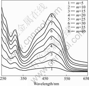
Fig.1 UV-vis absorption spectra of PDDA/PS-119 multilayer films (m denotes dipping cycle number or bilayer number)
The thickness of layer-by-layer assembled films can be approximately calculated from X-ray diffraction Kiessig curves[9,10]. Fig.2 shows a typical low angle X-ray diffractogram of an assembled PDDA/PS-119 multilayer film with a dipping cycle number at m being 10. The low angle X-ray diffractogram was obtained by using a Rigaku D/MAX-YB X-ray diffractometer (Cu Ka, l=0.154 058 nm).
The total thickness of the multilayer films can be calculated using the equation given in Ref. [10]:
 (1)
(1)
where D is the total thickness of the films, λ is the wavelength of the X-ray, θk and θk+1 (unit in radian) denote the angles of the two adjoining peaks, respectively.
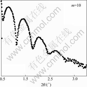
Fig.2 Low angle X-ray diffractogram of assembled PDDA/ PS-119 multilayer film (PDDA concentration: 1×10⁻³ mol/L; PS-119 concentration: 0.5 g/L; on silicon wafer)
If the dipping conditions are kept unchanged, the thickness of each PDDA/PS-119 bilayer should be almost the same.
Thus,
D=md (2)
where d is the average thickness of one PDDA/PS-119 bilayer.
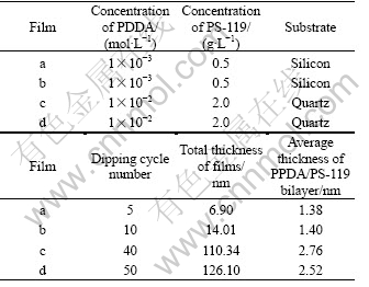
Table 1 lists the calculated values of the thickness of four layer-by-layer assembled PDDA/PS-119 films(a, b, c and d). The data indicate that the total thickness of the films is determined by the concentrations of the aqueous polyelectrolytes, and directly proportional to the dipping cycle number. The data also indicate that the average thickness of a monolayer of PDDA or PS-119 is around 1 nm, confirming that nanoscaled layers can be made with the layer-by-layer assembling process.
Table 1 Thickness of layer-by-layer assembled PDDA/PS-119 films
3.2 Copper phthalocyanine dye/colloidal cadmium sulfide particle films
CdS nanoparticle-based assembled multilayer films were prepared by different authors[11, 12]. In this study, the copper phthalocyanine dye we used was Alician Blue 8GX (AB). AB is a small organic molecule. The colloidal CdS particles are several nanometers in diameter as indicated in Fig.3. The HRTEM image was collected using a JEOL JEM 2010 FEF high-resolution transmission electron microscope at an acceleration voltage of 200 kV. The glass substrates were firstly dipped into the AB solution for 10 min, rinsed with ultrapure water and dried. Then, the substrates were dipped into colloidal CdS for 10 min, rinsed with ultrapure water and dried again. The absorption spectra were measured using a Shimadzu 2450 UV-vis spectrophotometer. Fig.4 shows the UV-vis absorption spectra of the AB/CdS films assembled on glass.

Fig.3 HRTEM image of colloidal CdS
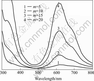
Fig.4 UV-vis absorption spectra of AB/CdS multiplayer films
The thickness of the thin films was measured with a Taylor Hobson Form Talysurf S4C nano profilometer. Fig.5 shows the thickness curve of a 20-bilayer film measured with the nano profilometer. On the curve, it can be observed that the total thickness of the film is about 500 nm. It should be noted that the dipping cycle number is only 20, which means that the average thickness of an AB/CdS bilayer is about 25 nm. So, this result is of notable interest. A reasonable explanation for the result is that both AB molecules and CdS particles aggregated in the film. However, it is found from the curve that, although there may be aggregation inside the film, the surface of the film is rather even. We have also made experiments using different organic molecules and colloidal particles, and found that AB and CdS are in pairs with really good assembling feature. Furthermore, we found that the AB/CdS films are of higher anti-scratching strength than other colloidal particle- based films. This experimental result indicates that small organic molecules and colloidal nanoparticles can be used to make layer-by-layer assembled films with thickness up to hundreds nanometers and that, to a great extent, the easiness to make the films depends on the assembling features of the precursor organic molecules and colloidal nanoparticles.

Fig.5 Thickness of 20-bilayer AB/CdS film measured with nano profilometer
3.3 Polyelectrolyte/multiwall carbon nanotube films
After the chemical treatment, MWCNT became water-soluble as the functional group ―COOH was introduced onto its surfaces. The water-soluble MWCNT can be alternatively assembled with polycations, such as poly(dimethylammonium chloride), poly(allylamine hydrochloride), polyethylenimine[13-15]. The polyelec- trolyte used in this experiment was polyethylenimine (PEI). PEI/CNTs multilayer films were also described by KOTOV et al[14, 15]. For PEI/MWCNT multilayer films, the layer-by-layer assembling process was similar to that for PDDA/PS-119 films except that the dipping time was 20 min and that the films were dried with hot air for a few minutes after each rinsing. Fig.6 shows the HRSEM images of a 60-bilayer PEI/MWCNT film. The images were taken with FEI sirion ultra-high resolution Schottky field emission scanning electron microscope, at the acceleration voltage of 20 kV. From Fig.6(b), it can be seen that the film is thicker than 900 nm. The average thickness of a bilayer is perhaps more than 15 nm. Obviously, for the PEI/MWCNT films, it is the MWCNT that makes the great contribution to the film thickness. The cross linking reactions between PEI and MWCNT could occur when the films were heated with hot air. The toughness of the films would be improved by such cross linking. In fact, the 60-bilayer PEI/MWCNT film could be peeled off from the glass substrate. Because the PEI/MWCNT films possess high toughness, it is expected that the PEI/MWCNT films could be used as novel substrates to prepare flexible sheet materials after being deposited or coated or doped with functional substances.
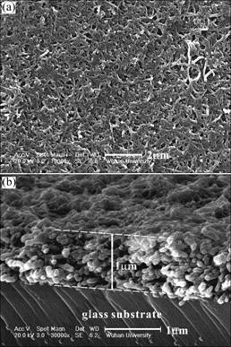
Fig.6 HRSEM images of 60-bilayer PEI/MWCNT film: (a) Out- most surface; (b) Cross section
4 Conclusions
The layer-by-layer assembling technique can be used to make ultrathin films, and the monolayer thickness of the assembled films can be controlled easily on nanometer scale. Usually, it is considered that to make “thick” films with this layer-by-layer assembling technique is time-consuming. However, these experi- ments demonstrated that, if suitable precursor materials are chosen, composite films with a thickness of hundreds of nanometers could be made in a relatively short time. In other words, it is not necessary to dip many cycles during film fabrication. For the organic molecule/ colloidal CdS films, a reasonable explanation for this result is that both the organic molecules and the CdS particles aggregate in the films. PEI/MWCNT films with a thickness of about 1 mm have been made. Obviously, it is the MWCNT that makes the great contribution to the film thickness.
References
[1] Decher G, Hong J D. Buildup of ultrathin multilayer films by a self-assembly process(II): consecutive adsorption of anionic and cationic bipolar amphiphiles and polyelectrolytes on charged surfaces [J]. Ber Bunsen Phys Chem, 1991, 95(11): 1430-1434.
[2] Decher G. Fuzzy nanoassemblies: toward layered polymeric multicomposites [J]. Science, 1997, 277: 1232-1237.
[3] ILER R K. Multilayers of colloidal particles [J]. J Colloid Interf Sci, 1966, 21(6): 569-594.
[4] FENDLER J H. Self-assembled nanostructured materials [J]. Chem Mater, 1996, 8(8): 1616-1624.
[5] Decher G, Schlenoff J B. Multilayer Thin Films: Sequential Assembly of Nanocomposite Materials [M]. Weinheim: Wiley-VCH, 2003.
[6] Jiang De-sheng, Li Hong-hui, Yu Hai-hu, Yang En-yu, Chen Xiao-yao, Li Xiao-fu. Preparation and spectral researches of CdS nanoparticles [J]. J Wuhan Univ Technol, 2005, 27(1): 7-9, 13.(in Chinese)
[7] Yu Hai-hu, Qin Lin-qing, Zhou Ling-de, Jiang De-sheng. Low angle XRD study on self-assembled polyelectrolyte multilayer films [J]. Chin J Colloid Polym, 2002, 20(3): 18-20, 10.(in Chinese)
[8] Yu Hai-hu, Jiang De-sheng. Ionic self-assembly and humidity sensitivity of polyelectrolyte multilayers [J]. Chin J Polymer Sci, 2002, 20(1): 1-7.
[9] Schmitt J, Grünewald T, Decher G, Pershan P S, Kjaer K, L?sche M. Internal structure of layer-by-layer adsorbed polyelectrolyte films: a neutron and X-ray reflectivity study [J]. Macromolecules, 1993, 26(25): 7058-7063.
[10] WU Zhi-qiang, Lu Xiang-dong, Huang Wen-yong, Liu Hong-tu, Jin Huai-cheng, Wang Chang-sui, Zhou Gui-en, Wu Zi-qin. Small-angle X-ray diffraction study of amorphous multilayer and single layer thin films [J]. Acta Phys Sin, 1987, 36(5): 591-598. (in Chinese)
[11] Kotov N A, Dékány I, Fendler J H. Layer-by-layer of electrolyte-semiconductor nanoparticle composite films [J]. J Phys Chem, 1995, 99(35): 13065- 13609.
[12] Yu Hai-hu, Jiang De-sheng, Yang En-yu, Li Hong-hui, Chen Xiao-yao, Zhou Ling-de. Electrostatic self-assembly and characterization of poly(p-phenylene vinylene)/CdS nanocomposite films [J]. Proc of SPIE, 2005, 5632: 312-316.
[13] Rouse J H, Lillehei P T. Electrostatic assembly of polymer/single walled carbon nanotube multilayer films [J]. Nano Letters, 2003, 3(1): 59-62.
[14] Mamedov A A, Kotov N A, Prato M, Guldi D, Wicksted J P, Hirsch A. Molecular design of strong single-wall carbon nanotube/polyelectrolyte multilayer composites [J]. Nature Materials, 2002, 1(3): 190-194.
[15] Olek M, Ostrander J, Jurga S, M?hwald H, Kotov N, Kempa K, Giersig M. Layer-by-layer assembled composites from multiwall carbon nanotubes with different morphologies [J]. Nano Letters, 2004, 4(10): 1889-1895.
Foundation item: Project(60537050) supported by the National Natural Science Foundation of China
Corresponding author: YU Hai-hu; Tel: +86-27-87651850-8004; E-mail: hhyu@mail.whut.edu.cn
(Edited by LONG Huai-zhong)